SSF2301 MOSFET Equivalente. Reemplazo. Hoja de especificaciones. Principales características
Número de Parte: SSF2301
Tipo de FET: MOSFET
Polaridad de transistor: P
ESPECIFICACIONES MÁXIMAS
Pdⓘ - Máxima disipación de potencia: 1.25 W
|Vds|ⓘ - Voltaje máximo drenador-fuente: 20 V
|Vgs|ⓘ - Voltaje máximo fuente-puerta: 12 V
|Id|ⓘ - Corriente continua de drenaje: 3 A
Tjⓘ - Temperatura máxima de unión: 150 °C
CARACTERÍSTICAS ELÉCTRICAS
trⓘ - Tiempo de subida: 18 nS
Cossⓘ - Capacitancia de salida: 75 pF
RDSonⓘ - Resistencia estado encendido drenaje a fuente: 0.09 Ohm
Encapsulados: SOT23
Búsqueda de reemplazo de SSF2301 MOSFET
- Selecciónⓘ de transistores por parámetros
SSF2301 datasheet
ssf2301.pdf
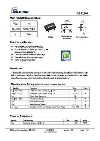
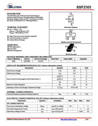
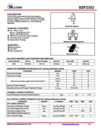
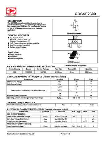
SSF2301 Main Product Characteristics D VDSS -20V G RDS(on) 60m (typ.) S ID -3A Marking and pin SOT-23 Schematic diagram Assignme nt Features and Benefits Advanced MOSFET process technology Special designed for PWM, load switching and general purpose applications Ultra low on-resistance with low gate charge Fast switching and reverse body re
ssf2301b.pdf
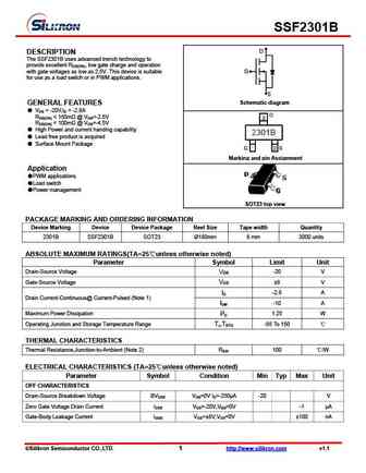
SSF2301B D DESCRIPTION The SSF2301B uses advanced trench technology to provide excellent RDS(ON), low gate charge and operation with gate voltages as low as 2.5V. This device is suitable G for use as a load switch or in PWM applications. S Schematic diagram GENERAL FEATURES VDS = -20V,ID = -2.8A RDS(ON)
ssf2301a.pdf
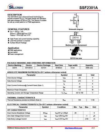
SSF2301A D DESCRIPTION The SSF2301A uses advanced trench technology to provide excellent RDS(ON), low gate charge and operation with gate voltages as low as 2.5V. This device is suitable G for use as a load switch or in PWM applications. S Schematic diagram GENERAL FEATURES VDS = -20V,ID = -4A RDS(ON)
ssf2300.pdf
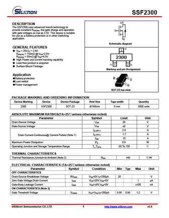
SSF2300 D DESCRIPTION The SSF2300 uses advanced trench technology to provide excellent RDS(ON), low gate charge and operation G with gate voltages as low as 2.5V. This device is suitable for use as a Battery protection or in other Switching application. S Schematic diagram GENERAL FEATURES VDS = 20V,ID = 2.4A RDS(ON)
Otros transistores... SSF2116EJ3, SSF2122E, SSF2129H3, SSF2145CH6, SSF2160G4, SSF2300, SSF2300A, SSF2300B, P55NF06, SSF2301A, SSF2301B, SSF2302, SSF2305, SSF2306, SSF2307B, SSF2312, SSF2314
History: CSD22204W
🌐 : EN ES РУ

Liste
Recientemente añadidas las descripciónes de los transistores:
MOSFET: FTF30P35D | FTF25N35DHVT | FTF15N35D | FTE15C35G | FTP02P15G | FTE02P15G | AKF30N5P0SX | AKF30N10S | AKF20P45D | CM4407 | CM3407 | CM3400 | SVF11N65F | SVF11N65T | FKBB3105 | EHBA036R1
Popular searches
2n5485 equivalent | 2sa1941 | 2sc485 | 2sd287 | 2sd438 | a1492 | hy4008 | ncep039n10m