SSF2485 MOSFET Equivalente. Reemplazo. Hoja de especificaciones. Principales características
Número de Parte: SSF2485
Tipo de FET: MOSFET
Polaridad de transistor: P
ESPECIFICACIONES MÁXIMAS
Pdⓘ - Máxima disipación de potencia: 1.1 W
|Vds|ⓘ - Voltaje máximo drenador-fuente: 20 V
|Vgs|ⓘ - Voltaje máximo fuente-puerta: 10 V
|Id|ⓘ - Corriente continua de drenaje: 3 A
Tjⓘ - Temperatura máxima de unión: 150 °C
CARACTERÍSTICAS ELÉCTRICAS
trⓘ - Tiempo de subida: 15 nS
Cossⓘ - Capacitancia de salida: 65 pF
RDSonⓘ - Resistencia estado encendido drenaje a fuente: 0.1 Ohm
Encapsulados: SOT23-6
Búsqueda de reemplazo de SSF2485 MOSFET
- Selecciónⓘ de transistores por parámetros
SSF2485 datasheet
ssf2485.pdf
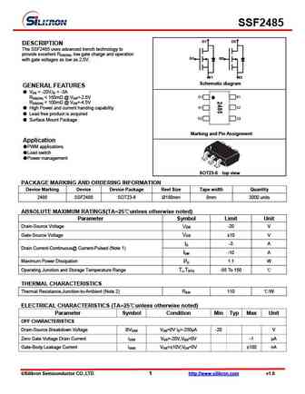
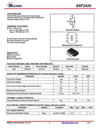
SSF2485 D1 D2 DESCRIPTION The SSF2485 uses advanced trench technology to provide excellent RDS(ON), low gate charge and operation G1 G2 with gate voltages as low as 2.5V. S1 S2 Schematic diagram GENERAL FEATURES VDS = -20V,ID = -3A RDS(ON)
ssf2418eb.pdf
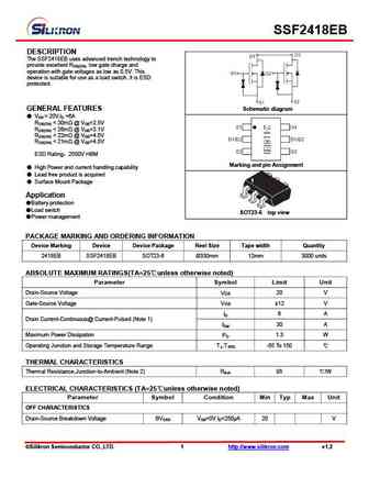
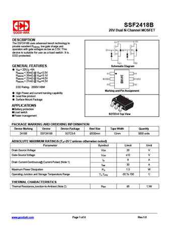
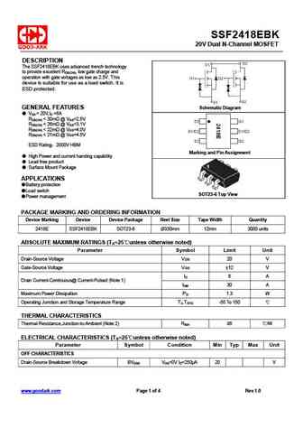
SSF2418EB DESCRIPTION The SSF2418EB uses advanced trench technology to provide excellent RDS(ON), low gate charge and operation with gate voltages as low as 0.5V. This device is suitable for use as a load switch. It is ESD protected. Schematic diagram GENERAL FEATURES VDS = 20V,ID =6A RDS(ON)
ssf2418e.pdf
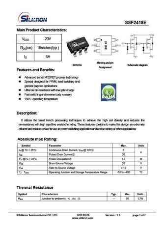
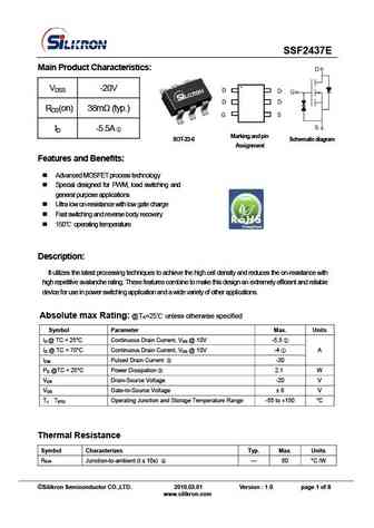
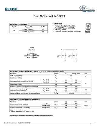
SSF2418E Main Product Characteristics VDSS 20V RDS(on) 18mohm(typ.) ID 6A Mark ing an d pi n SOT23-6 Schema t ic diagr a m Assignment Features and Benefits Advanced trench MOSFET process technology Special designed for PWM, load switching and general purpose applications Ultra low on-resistance with low gate charge Fast switching and reverse body re
ssf2449.pdf
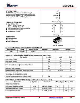
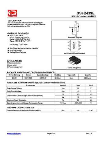
SSF2449 D DESCRIPTION The SSF2449 uses advanced trench technology to provide excellent RDS(ON), low gate charge and operation with gate voltages as low as 2.5V. This device is suitable G for use as a load switch or in PWM applications. S Schematic diagram GENERAL FEATURES VDS = -20V,ID = -5A RDS(ON)
Otros transistores... SSF2336, SSF2341E, SSF2356G8, SSF2418E, SSF2418EB, SSF2429, SSF2437E, SSF2449, K4145, SSF2610E, SSF2616E, SSF2627, SSF2637E, SSF2649, SSF26NS60, SSF26NS60A, SSF2701
🌐 : EN ES РУ

Liste
Recientemente añadidas las descripciónes de los transistores:
MOSFET: FTF30P35D | FTF25N35DHVT | FTF15N35D | FTE15C35G | FTP02P15G | FTE02P15G | AKF30N5P0SX | AKF30N10S | AKF20P45D | CM4407 | CM3407 | CM3400 | SVF11N65F | SVF11N65T | FKBB3105 | EHBA036R1
Popular searches
2sd551 | ac128 datasheet | 2n5496 | 2sb600 | 2sa1209 | 2sc1364 replacement | 2sd665 | 7506 mosfet datasheet