SSF3338 MOSFET Equivalente. Reemplazo. Hoja de especificaciones. Principales características
Número de Parte: SSF3338
Tipo de FET: MOSFET
Polaridad de transistor: N
ESPECIFICACIONES MÁXIMAS
Pdⓘ - Máxima disipación de potencia: 1.25 W|Vds|ⓘ - Voltaje máximo drenador - fuente: 30 V
|Vgs|ⓘ - Voltaje máximo fuente - puerta: 20 V
|Id|ⓘ - Corriente continua de drenaje: 4 A
Tjⓘ - Temperatura máxima de unión: 150 °C
CARACTERÍSTICAS ELÉCTRICAS
trⓘ - Tiempo de subida: 12 nS
Cossⓘ - Capacitancia de salida: 60 pF
Rds(on)ⓘ - Resistencia estado encendido drenaje a fuente: 0.047 Ohm
Paquete / Cubierta: SOT23
Búsqueda de reemplazo de SSF3338 MOSFET
SSF3338 datasheet
ssf3338.pdf
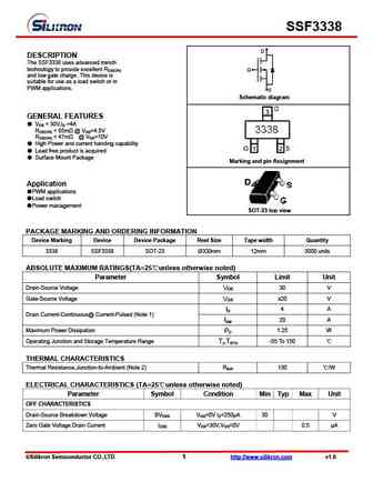
SSF3338 D DESCRIPTION The SSF3338 uses advanced trench technology to provide excellent RDS(ON) G and low gate charge .This device is suitable for use as a load switch or in PWM applications. S Schematic diagram GENERAL FEATURES VDS = 30V,ID =4A RDS(ON)
ssf3339.pdf
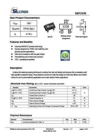
SSF3339 Main Product Characteristics D VDSS -30V G RDS(on) 37m (typ.) S ID -4.1A Marking and pin SOT-23 Schematic diagram Assignme nt Features and Benefits Advanced MOSFET process technology Special designed for PWM, load switching and general purpose applications Ultra low on-resistance with low gate charge Fast switching and reverse body
ssf3341.pdf
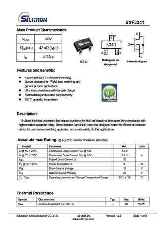
SSF3341 Main Product Characteristics D VDSS -30V G RDS(on) 42m (typ.) S ID -4.2A Marking and pin SOT-23 Schematic diagram Assignme nt Features and Benefits Advanced MOSFET process technology Special designed for PWM, load switching and general purpose applications Ultra low on-resistance with low gate charge Fast switching and reverse body
ssf3341l.pdf

SSF3341L D DESCRIPTION The SSF3341L uses advanced trench technology to provide excellent RDS(ON), low gate charge and operation with gate voltages as low as 2.5V. This device is suitable G for use as a load switch or in PWM applications. S GENERAL FEATURES Schematic diagram VDS = -30V,ID = -4.2A RDS(ON)
Otros transistores... SSF3055 , SSF3056C , SSF3092G1 , SSF3117 , SSF32E0E , SSF3314E , SSF3322 , SSF3324 , P60NF06 , SSF3339 , SSF3341 , SSF3341L , SSF3365 , SSF3402 , SSF3416 , SSF3420 , SSF3428 .
History: MMBFJ310

History: MMBFJ310


Liste
Recientemente añadidas las descripciónes de los transistores:
MOSFET: AOK065V65X2 | AOK065V120X2 | AOK033V120X2Q | AOK033V120X2 | AOB380A60L | AOB29S50L | AO3481C | AO3480 | APG068N04Q | APG068N04G | APG060N85D | APG054N10D | APG054N10 | APG050N85D | APG050N85 | APG046N01G
Popular searches
2sc1328 | 2sc1845 transistor | a933 transistor datasheet | a1633 transistor | 2sa844 | 2sc1327 | 2sc3855 | 2sc945 transistor equivalent