APM4953K MOSFET Equivalente. Reemplazo. Hoja de especificaciones. Principales características
Número de Parte: APM4953K
Tipo de FET: MOSFET
Polaridad de transistor: P
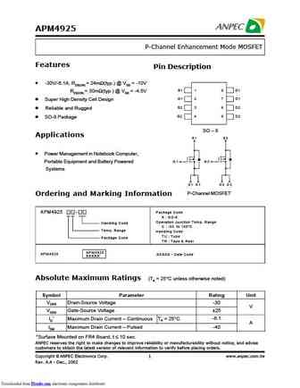
ESPECIFICACIONES MÁXIMAS
Pdⓘ - Máxima disipación de potencia: 2 W
|Vds|ⓘ - Voltaje máximo drenador-fuente: 30 V
|Vgs|ⓘ - Voltaje máximo fuente-puerta: 25 V
|Id|ⓘ - Corriente continua de drenaje: 4.9 A
Tjⓘ - Temperatura máxima de unión: 150 °C
CARACTERÍSTICAS ELÉCTRICAS
trⓘ - Tiempo de subida: 15 nS
Cossⓘ - Capacitancia de salida: 400 pF
RDSonⓘ - Resistencia estado encendido drenaje a fuente: 0.06 Ohm
Encapsulados: SOP8
Búsqueda de reemplazo de APM4953K MOSFET
- Selecciónⓘ de transistores por parámetros
APM4953K datasheet
apm4953k.pdf

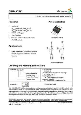
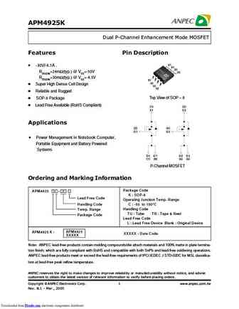
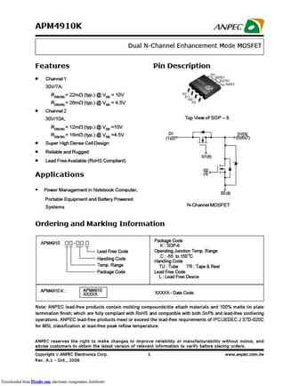
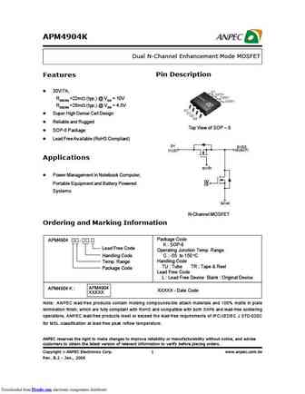
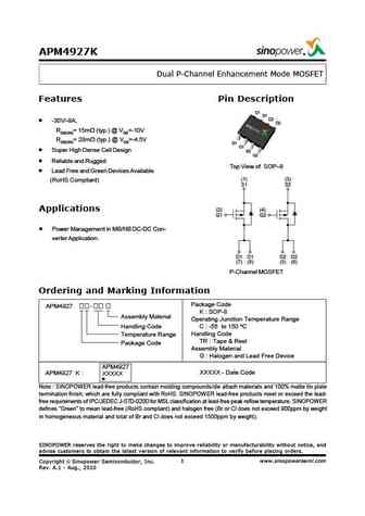
APM4953K Dual P-Channel Enhancement Mode MOSFET Features Pin Description D1 D1 -30V/-4.9A , D2 D2 RDS(ON)=53m (typ.) @ VGS=-10V RDS(ON)=80m (typ.) @ VGS=-4.5V S1 Reliable and Rugged G1 S2 G2 ESD Protection Top View of SOP 8 Lead Free and Green Devices Available (RoHS Compliant) (1) (3) S1 S2 Applications (2) (4) G1 G2 Power Management in Notebook Computer, Po
apm4953k.pdf
APM4953K Dual P-Channel Enhancement Mode MOSFET Features Pin Description D1 D1 -30V/-4.9A , D2 D2 RDS(ON)=53m (typ.) @ VGS=-10V RDS(ON)=80m (typ.) @ VGS=-4.5V S1 Reliable and Rugged G1 S2 G2 ESD Protection Top View of SOP 8 Lead Free and Green Devices Available (RoHS Compliant) (1) (3) S1 S2 Applications (2) (4) G1 G2 Power Management in Notebook Computer, Po
apm4953kc.pdf
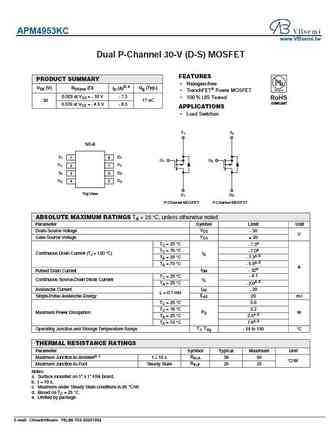
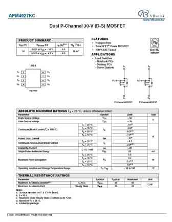
APM4953KC www.VBsemi.tw Dual P-Channel 30-V (D-S) MOSFET FEATURES PRODUCT SUMMARY Halogen-free VDS (V) RDS(on) ( ) ID (A)d, e Qg (Typ.) TrenchFET Power MOSFET 0.029 at VGS = - 10 V - 7.3 100 % UIS Tested RoHS - 30 17 nC COMPLIANT 0.039 at VGS = - 4.5 V - 6.3 APPLICATIONS Load Switches S1 S2 SO-8 S1 1 D1 8 G1 G2 G1 2 D1 7 S2 3 D2 6 G2 4 D2 5 Top Vi
apm4953.pdf
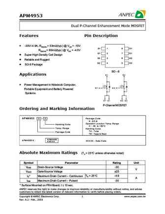
APM4953 Dual P-Channel Enhancement Mode MOSFET Features Pin Description -30V/-4.9A, RDS(ON) = 53m (typ.) @ VGS = -10V S1 1 8 D1 RDS(ON) = 80m (typ.) @ VGS = -4.5V G1 2 7 D1 Super High Density Cell Design S2 3 6 D2 Reliable and Rugged G2 45 D2 SO-8 Package SO - 8 Applications S1 S2 Power Managemen

Otros transistores... APM4835 , APM4904K , APM4906K , APM4910K , APM4925 , APM4925K , APM4947K , APM4953 , IRFP450 , APM7312 , APM7312K , APM7313K , APM7314 , APM7314K , APM7316 , APM7318 , APM7318K .
History: SI2318DS-T1-GE3 | H2301N | FCPF190N65S3R0L | S68N08RP | S70N06RP | AGM4025D
History: SI2318DS-T1-GE3 | H2301N | FCPF190N65S3R0L | S68N08RP | S70N06RP | AGM4025D
🌐 : EN ES РУ

Liste
Recientemente añadidas las descripciónes de los transistores:
MOSFET: AUB062N08BG | AUB060N08AG | AUB056N10 | AUB056N08BGL | AUB050N085 | AUB050N055 | AUB045N12 | AUB045N10BT | AUB039N10 | AUB034N10 | AUB033N08BG | AUB026N085 | AUA062N08BG | AUA060N08AG | AUA056N08BGL | AUA039N10
Popular searches
2sc828 replacement | 2sd669 datasheet | c102 transistor | bt152 datasheet | 2sa1302 datasheet | mpsa13 transistor equivalent | кт817г характеристики | 2sc1972