8822 Datasheet. Equivalente. Reemplazo. Hoja de especificaciones. Principales características
Número de Parte: 8822 📄📄
Tipo de FET: MOSFET
Polaridad de transistor: N
ESPECIFICACIONES MÁXIMAS
Pdⓘ - Máxima disipación de potencia: 1.5 W
|Vds|ⓘ - Voltaje máximo drenador-fuente: 20 V
|Vgs|ⓘ - Voltaje máximo fuente-puerta: 10 V
|Id|ⓘ - Corriente continua de drenaje: 6 A
Tjⓘ - Temperatura máxima de unión: 150 °C
CARACTERÍSTICAS ELÉCTRICAS
RDSonⓘ - Resistencia estado encendido drenaje a fuente: 0.022 Ohm
Encapsulados: TSSOP8
📄📄 Copiar
Búsqueda de reemplazo de 8822 MOSFET
- Selecciónⓘ de transistores por parámetros
8822 datasheet
..1. Size:556K shenzhen
8822.pdf 
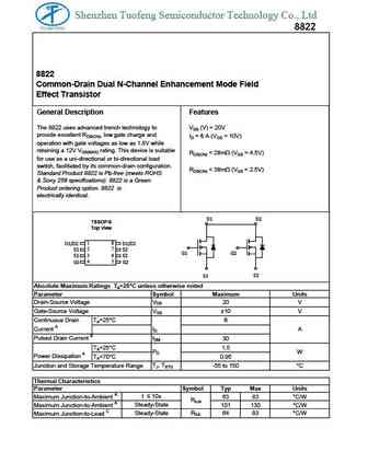
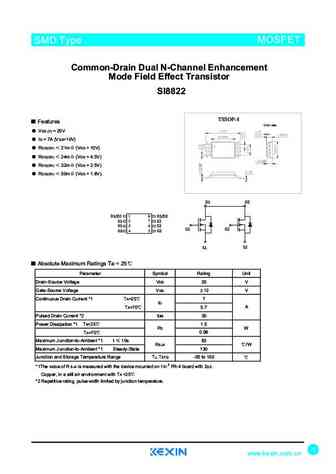
Shenzhen Tuofeng Semiconductor Technology Co., Ltd 8822 8822 Common-Drain Dual N-Channel Enhancement Mode Field Effect Transistor General Description Features The 8822 uses advanced trench technology to VDS (V) = 20V provide excellent RDS(ON), low gate charge and ID = 6 A (VGS = 10V) operation with gate voltages as low as 1.8V while retaining a 12V VGS(MAX) rating. This device is
0.2. Size:150K diodes
dmg8822uts.pdf
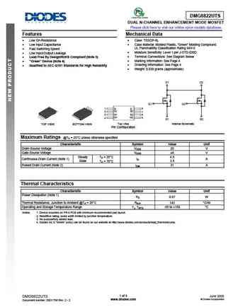
DMG8822UTS DUAL N-CHANNEL ENHANCEMENT MODE MOSFET Please click here to visit our online spice models database. Features Mechanical Data Low On-Resistance Case TSSOP-8L Low Input Capacitance Case Material Molded Plastic, Green Molding Compound. UL Flammability Classification Rating 94V-0 Fast Switching Speed Moisture Sensitivity Level 1 per J-STD-020
0.3. Size:2155K htsemi
pt8822.pdf
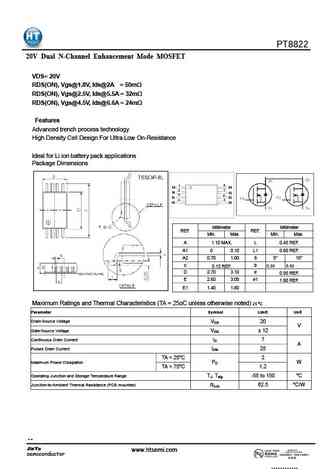
PT8822 20V Dual N-Channel Enhancement Mode MOSFET VDS= 20V RDS(ON), Vgs@1.8V, Ids@2A = 50m RDS(ON), Vgs@2.5V, Ids@5.5A = 32m RDS(ON), Vgs@4.5V, Ids@6.6A = 24m Features Advanced trench process technology High Density Cell Design For Ultra Low On-Resistance Ideal for Li ion battery pack applications Package Dimensions 1 8 D1 D2 2 7 S1 S2 3 6 S1 S2 4 5 G1 G2
0.4. Size:197K aosemi
ao8822.pdf
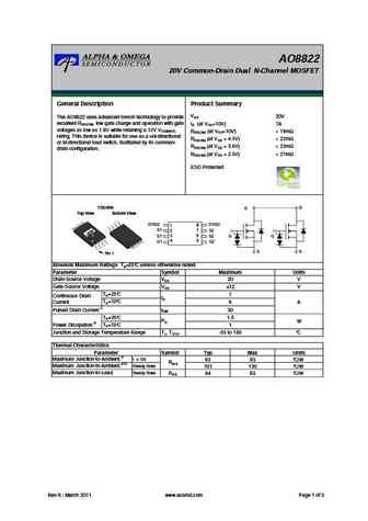
AO8822 20V Common-Drain Dual N-Channel MOSFET General Description Product Summary VDS 20V The AO8822 uses advanced trench technology to provide excellent RDS(ON), low gate charge and operation with gate ID (at VGS=10V) 7A voltages as low as 1.8V while retaining a 12V VGS(MAX) RDS(ON) (at VGS=10V)
0.5. Size:691K alfa-mos
afn8822s.pdf
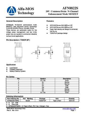
AFN8822S Alfa-MOS 20V Common-Drain N-Channel Technology Enhancement Mode MOSFET General Description Features AFN8822S, N-Channel enhancement mode 20V/6.5A,RDS(ON)=32m @VGS=4.5V MOSFET, uses Advanced Trench Technology 20V/4.8A,RDS(ON)=35m @VGS=2.5V to provide excellent RDS(ON), low gate charge. Super high density cell design for extremely These devices are particul
0.6. Size:691K alfa-mos
afn8822.pdf
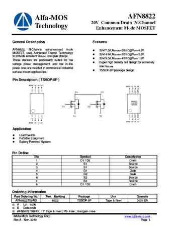
AFN8822 Alfa-MOS 20V Common-Drain N-Channel Technology Enhancement Mode MOSFET General Description Features AFN8822, N-Channel enhancement mode 20V/7.2A,RDS(ON)=28m @VGS=4.5V MOSFET, uses Advanced Trench Technology 20V/4.8A,RDS(ON)=32m @VGS=2.5V to provide excellent RDS(ON), low gate charge. 20V/3.0A,RDS(ON)=45m @VGS=1.8V These devices are particularly suited fo
0.7. Size:304K silikron
ssf8822.pdf
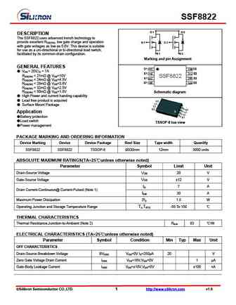
SSF8822 D1 D2 DESCRIPTION The SSF8822 uses advanced trench technology to provide excellent RDS(ON), low gate charge and operation G1 G2 with gate voltages as low as 0.8V. This device is suitable for use as a uni-directional or bi-directional load switch, S1 S2 facilitated by its common-drain configuration. Marking and pin Assignment GENERAL FEATURES V = 20V,I = 7A DS
0.8. Size:266K first silicon
ftk8822.pdf
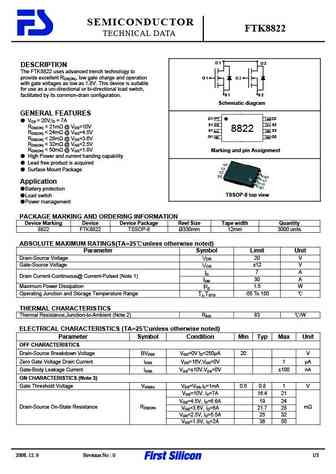
SEMICONDUCTOR FTK8822 TECHNICAL DATA D 1 D 2 DESCRIPTION The FTK8822 uses advanced trench technology to provide excellent RDS(ON), low gate charge and operation G 1 G 2 with gate voltages as low as 1.8V. This device is suitable for use as a uni-directional or bi-directional load switch, S 1 S 2 facilitated by its common-drain configuration. Schematic diagram GENERAL FEATURES
0.9. Size:135K kexin
ko8822.pdf
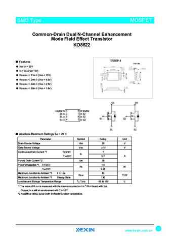
SMD Type IC SMD Type MOSFET Common-Drain Dual N-Channel Enhancement Mode Field Effect Transistor KO8822 TSSOP-8 Features Unit mm VDS (V) = 20V ID = 7A (VGS=10V) RDS(ON) 21m (VGS = 10V) RDS(ON) 24m (VGS = 4.5V) RDS(ON) 32m (VGS = 2.5V) RDS(ON) 50m (VGS = 1.8V) D1 D2 D1/D2 1 8 D1/D2 2 7 S1 S2 3 6 S1 S2 G1 G2 4 5 G1
0.10. Size:1801K elm
elm588822a-s.pdf
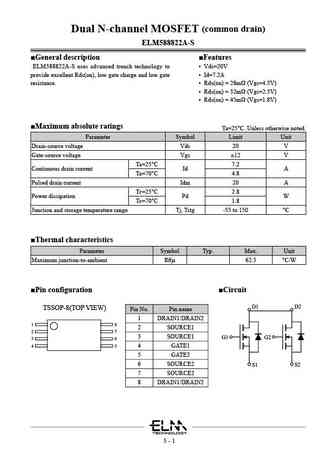
(common drain) Dual N-channel MOSFET ELM588822A-S General description Features ELM588822A-S uses advanced trench technology to Vds=20V provide excellent Rds(on), low gate charge and low gate Id=7.2A resistance. Rds(on) = 28m (Vgs=4.5V) Rds(on) = 32m (Vgs=2.5V) Rds(on) = 45m (Vgs=1.8V) Maximum absolute ratings Ta=25 C. Unless otherwise noted. Par
0.11. Size:1270K elm
elm58822sa.pdf
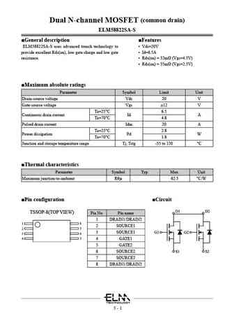
(common drain) Dual N-channel MOSFET ELM58822SA-S General description Features ELM58822SA-S uses advanced trench technology to Vds=20V provide excellent Rds(on), low gate charge and low gate Id=6.5A resistance. Rds(on) = 32m (Vgs=4.5V) Rds(on) = 35m (Vgs=2.5V) Maximum absolute ratings Parameter Symbol Limit Unit Drain-source voltage Vds 20 V Gate-sourc
0.12. Size:395K elm
elm18822ba.pdf
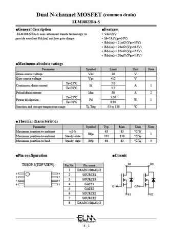
(common drain) Dual N-channel MOSFET ELM18822BA-S General description Features ELM18822BA-S uses advanced trench technology to Vds=20V provide excellent Rds(on) and low gate charge. Id=7A (Vgs=10V) Rds(on)
0.13. Size:439K globaltech semi
gsm8822.pdf
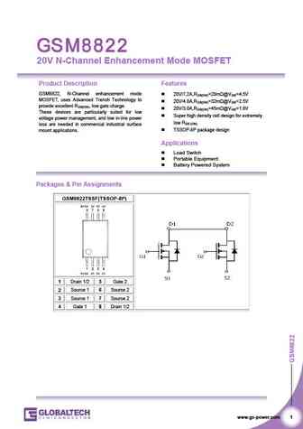
20V N-Channel Enhancement Mode MOSFET Product Description Features GSM8822, N-Channel enhancement mode 20V/7.2A,RDS(ON)=28m @VGS=4.5V MOSFET, uses Advanced Trench Technology to 20V/4.8A,RDS(ON)=32m @VGS=2.5V provide excellent RDS(ON), low gate charge. 20V/3.0A,RDS(ON)=45m @VGS=1.8V These devices are particularly suited for low Super high density cell desig
0.14. Size:432K globaltech semi
gsm8822s.pdf
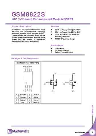
20V N-Channel Enhancement Mode MOSFET Product Description Features GSM8822S, N-Channel enhancement mode 20V/6.5A,RDS(ON)=32m @VGS=4.5V MOSFET, uses Advanced Trench Technology 20V/4.8A,RDS(ON)=35m @VGS=2.5V to provide excellent RDS(ON), low gate charge. Super high density cell design for These devices are particularly suited for low extremely low RDS (ON) volt
0.15. Size:154K m-mos
mmn8822.pdf
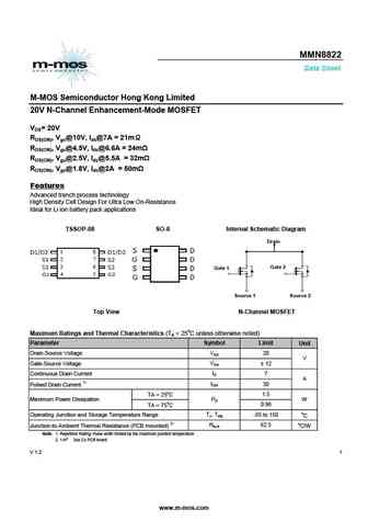
MMN8822 Data Sheet M-MOS Semiconductor Hong Kong Limited 20V N-Channel Enhancement-Mode MOSFET VDS= 20V RDS(ON), Vgs@10V, Ids@7A = 21m RDS(ON), Vgs@4.5V, Ids@6.6A = 24m RDS(ON), Vgs@2.5V, Ids@5.5A = 32m RDS(ON), Vgs@1.8V, Ids@2A = 50m Features Advanced trench process technology High Density Cell Design For Ultra Low On-Resistance Ideal for Li ion battery pack application
0.16. Size:610K stansontech
stn8822.pdf
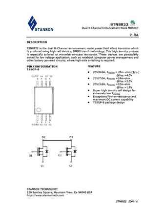
STN8822 Dual N Channel Enhancement Mode MOSFET 8.0A DESCRIPTION STN8822 is the dual N-Channel enhancement mode power field effect transistor which is produced using high cell density, DMOS trench technology. This high density process is especially tailored to minimize on-state resistance. These devices are particularly suited for low voltage application, such as notebook computer
0.17. Size:734K stansontech
stn8822a.pdf
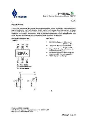
STN8822A Dual N Channel Enhancement Mode MOSFET 6.0A DESCRIPTION STN8822A is the dual N-Channel enhancement mode power field effect transistor which is produced using high cell density, DMOS trench technology. This high density process is especially tailored to minimize on-state resistance. These devices are particularly suited for low voltage application, such as notebook comput
Otros transistores... 4812, 4835, 4920, 4946, 4953, 6604, 8810, 8820, AON7506, 9435, 4953A, 4953B, 9926A, 9926B, AO3410, APM2317, FDMA905