50N03 MOSFET Equivalente. Reemplazo. Hoja de especificaciones. Principales características
Número de Parte: 50N03
Tipo de FET: MOSFET
Polaridad de transistor: N
ESPECIFICACIONES MÁXIMAS
Pdⓘ - Máxima disipación de potencia: 60 W
|Vds|ⓘ - Voltaje máximo drenador-fuente: 30 V
|Vgs|ⓘ - Voltaje máximo fuente-puerta: 20 V
|Id|ⓘ - Corriente continua de drenaje: 50 A
Tjⓘ - Temperatura máxima de unión: 175 °C
CARACTERÍSTICAS ELÉCTRICAS
Cossⓘ - Capacitancia de salida: 280 pF
RDSonⓘ - Resistencia estado encendido drenaje a fuente: 0.0065 Ohm
Encapsulados: TO252
Búsqueda de reemplazo de 50N03 MOSFET
- Selecciónⓘ de transistores por parámetros
50N03 datasheet
50n03.pdf
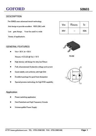
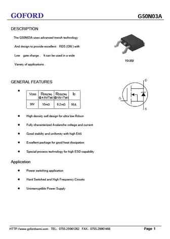
GOFORD 50N03 DESCRIPTION The 50N03 uses advanced trench technology VDS RDS(ON) ID And design to provide excellent RDS (ON ) with 30V -- 50A Low gate charge . It can be used in a wide Vanety of applications . GENERAL FEATURES VDS = 30 V, ID = 50 A TO-252 RDS(ON)
gl150n03ad.pdf
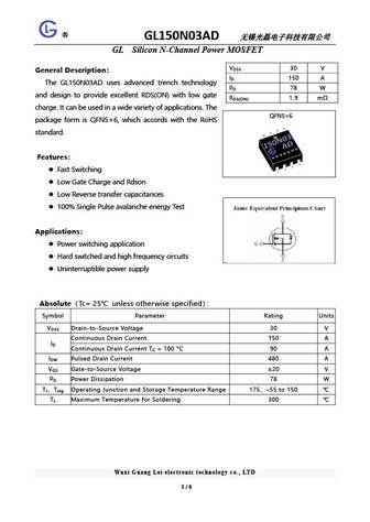
R GL150N03AD GL Silicon N-Channel Power MOSFET V 30 V DSS General Description ID 150 A The GL150N03AD uses advanced trench technology P 78 W D and design to provide excellent RDS(ON) with low gate R 1.9 m DS(ON) charge. It can be used in a wide variety of applications. The QFN5 6 package form is QFN5 6, which accord
msk50n03df.pdf
www.msksemi.com MSK50N03DF Semiconductor Compiance Description D D D D The MSK50N03DF is the high cell density trenched N-ch MOSFETs, which provide excellent RDSON and gate charge for most of the synchronous buck converter applications. S S S G The MSK50N03DF meet the RoHS and Green DFN3X3-8L Product Summary BVDSS RDSON ID 30V 46A 9.5m Green Device Available Super Low Gate
cjac150n03.pdf
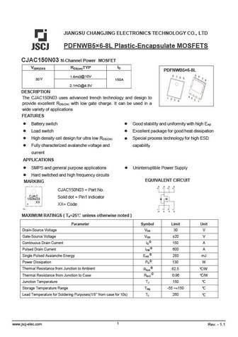
JIANGSU CHANGJING ELECTRONICS TECHNOLOGY CO., LTD PDFN 5 6-8L Plastic-Encapsulate MOSFETS CJAC150N03 N-Channel Power MOSFET ID V(BR)DSS RDS(on)TYP PDFN 5 6-8L 1.6m @10V 30 V 150A 2.1m @4.5V DESCRIPTION 15 FEATURES
phb50n03lt phd50n03lt php50n03lt 7.pdf
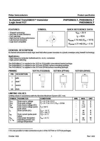
Philips Semiconductors Product specification N-channel TrenchMOS transistor PHP50N03LT, PHB50N03LT Logic level FET PHD50N03LT FEATURES SYMBOL QUICK REFERENCE DATA Trench technology d VDSS = 25 V Very low on-state resistance Fast switching ID = 48 A High thermal cycling performance Low thermal resistance RDS(ON) 16 m (VGS = 10 V) g Logic leve
phb50n03t 1.pdf
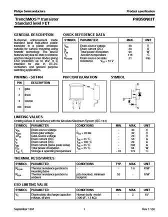
Philips Semiconductors Product specification TrenchMOS transistor PHB50N03T Standard level FET GENERAL DESCRIPTION QUICK REFERENCE DATA N-channel enhancement mode SYMBOL PARAMETER MAX. UNIT standard level field-effect power transistor in a plastic envelope VDS Drain-source voltage 30 V suitable for surface mounting using ID Drain current (DC) 50 A trench technology. The devic
php50n03t 1.pdf
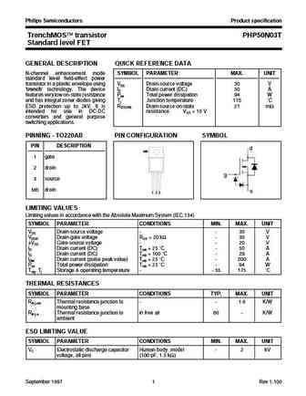
Philips Semiconductors Product specification TrenchMOS transistor PHP50N03T Standard level FET GENERAL DESCRIPTION QUICK REFERENCE DATA N-channel enhancement mode SYMBOL PARAMETER MAX. UNIT standard level field-effect power transistor in a plastic envelope using VDS Drain-source voltage 30 V trench technology. The device ID Drain current (DC) 50 A features very low on-state r
std50n03l std50n03l-1.pdf
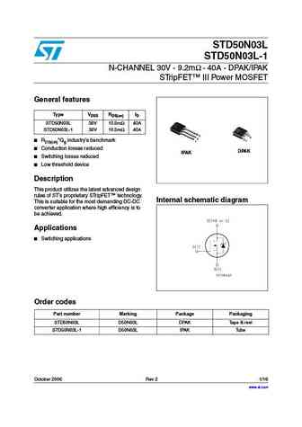
STD50N03L STD50N03L-1 N-CHANNEL 30V - 9.2m - 40A - DPAK/IPAK STripFET III Power MOSFET General features Type VDSS RDS(on) ID STD50N03L 30V 10.5m 40A STD50N03L-1 30V 10.5m 40A 3 3 2 RDS(on)*Qg industry s benchmark 1 1 Conduction losses reduced DPAK IPAK Switching losses reduced Low threshold device Description This product utilizes the latest advan
fdd050n03b.pdf
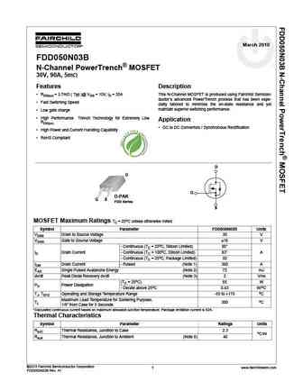
March 2010 FDD050N03B N-Channel PowerTrench MOSFET 30V, 90A, 5m Features Description RDS(on) = 3.7m ( Typ.)@ VGS = 10V, ID = 25A This N-Channel MOSFET is produced using Fairchild Semicon- ductor s advanced PowerTrench process that has been espe- Fast Switching Speed cially tailored to minimize the on-state resistance and yet maintain superior switching performance.
rmw150n03.pdf
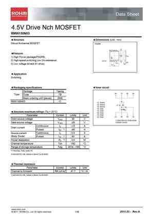
Data Sheet 4.5V Drive Nch MOSFET RMW150N03 Structure Dimensions (Unit mm) Silicon N-channel MOSFET PSOP8 (8) (7) (6) (5) Features 0 0.1 1) High Power package(PSOP8). 2) High-speed switching,Low On-resistance. 1pin mark (1) (2) (3) (4) 0.22 0.4 3) Low voltage drive(4.5V drive). 0.9 1.27 5.0 Application Switching Packaging specifications Inner circuit
sum50n03-13lc.pdf
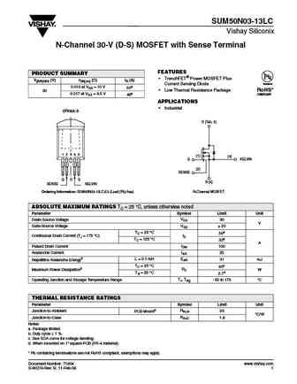
SUM50N03-13LC Vishay Siliconix N-Channel 30-V (D-S) MOSFET with Sense Terminal FEATURES PRODUCT SUMMARY TrenchFET Power MOSFET Plus V(BR)DSS (V) rDS(on) ( )ID (A) Available Current Sensing Diode 0.013 at VGS = 10 V 50a Low Thermal Resistance Package RoHS* 30 0.017 at VGS = 4.5 V COMPLIANT 48a APPLICATIONS Industrial D2PAK-5 D (Tab, 3) 1 2 3 4 5 (1) (4)
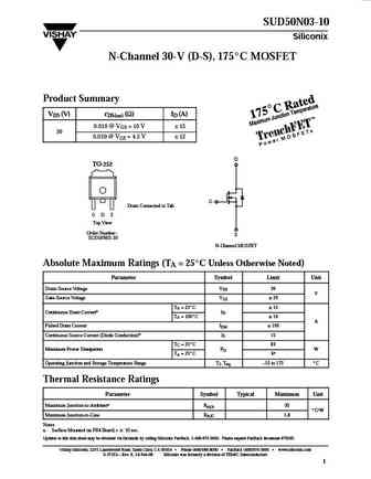
sud50n03-07.pdf
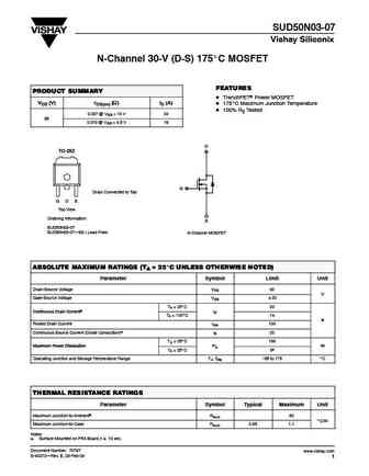
SUD50N03-07 Vishay Siliconix N-Channel 30-V (D-S) 175_C MOSFET FEATURES PRODUCT SUMMARY D TrenchFETr Power MOSFET VDS (V) rDS(on) (W) ID (A) D 175_C Maximum Junction Temperature D 100% Rg Tested 0.007 @ VGS = 10 V 20 30 30 0.010 @ VGS = 4.5 V 16 D TO-252 G Drain Connected to Tab G D S Top View Ordering Information S SUD50N03-07 SUD50N03-07 E3 ( Lead Free) N-Channel MOS
suu50n03.pdf
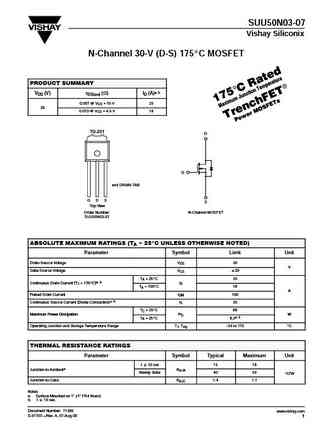
SUU50N03-07 Vishay Siliconix N-Channel 30-V (D-S) 175_CMOSFET PRODUCT SUMMARY VDS (V) rDS(on) ( ) ID (A)a, b 0.007 @ VGS =10V 25 30 30 0.010 @ VGS =4.5V 18 TO-251 D G and DRAIN-TAB G D S S Top View Order Number N-Channel MOSFET SUU50N03-07 ABSOLUTE MAXIMUM RATINGS (TA = 25_C UNLESS OTHERWISE NOTED) Parameter Symbol Limit Unit Drain-Source Voltage VDS 30 V V Gate-Source
sud50n03-11.pdf
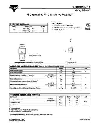
SUD50N03-11 Vishay Siliconix N-Channel 30-V (D-S) 175 C MOSFET FEATURES PRODUCT SUMMARY TrenchFET Power MOSFET VDS (V) RDS(on) ( ) ID (A)a 175 C Maximum Junction Temperature RoHS 0.011 at VGS = 10 V 50 COMPLIANT 30 100 % Rg Tested 0.017 at VGS = 4.5 V 43 D TO-252 G Drain Connected to Tab G D S S Top View Ordering Information SUD50N03-11-E3 (Lead
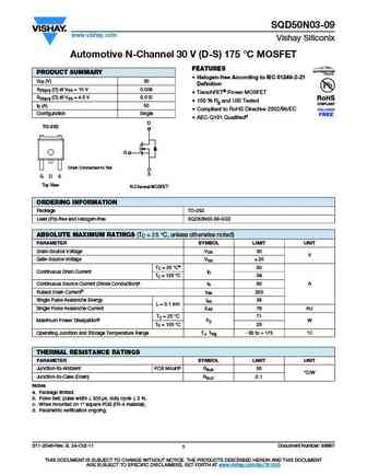
sqd50n03-4m0l.pdf
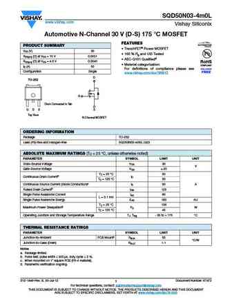
SQD50N03-4m0L www.vishay.com Vishay Siliconix Automotive N-Channel 30 V (D-S) 175 C MOSFET FEATURES PRODUCT SUMMARY TrenchFET Power MOSFET VDS (V) 30 100 % Rg and UIS Tested RDS(on) ( ) at VGS = 10 V 0.0031 AEC-Q101 Qualifiedd RDS(on) ( ) at VGS = 4.5 V 0.0040 Material categorization ID (A) 50 For definitions of compliance please see Configuration Single
sup50n03.pdf
SUP50N03-5m1P Vishay Siliconix N-Channel 30 V (D-S) MOSFET FEATURES PRODUCT SUMMARY Halogen-free According to IEC 61249-2-21 VDS (V) RDS(on) ( ) ID (A) Qg (Typ.) Definition 0.0051 at VGS = 10 V 50d TrenchFET Power MOSFET 30 21.7 0.0063 at VGS = 4.5 V 50d 100 % Rg and UIS Tested Compliant to RoHS Directive 2002/95/EC APPLICATIONS Power Supply - Seco
sud50n03-06p.pdf
SUD50N03-06P Vishay Siliconix N-Channel 30-V (D-S) 175 _C MOSFET FEATURES PRODUCT SUMMARY D TrenchFETr Power MOSFET D 175 _C Junction Temperature VDS (V) rDS(on) (W) ID (A)b D Optimized for Low-Side Synchronous Rectifier * Operation 0.0065 at VGS = 10 V 84b 30 30 D 100 % Rg Tested 0.0095 at VGS = 4.5 V 59b APPLICATIONS D DC/DC Converters D Synchronous Rectifiers TO-252 D Dr
sud50n03-7m3p.pdf
SUD50N03-7m3P New Product Vishay Siliconix N-Channel 30-V (D-S) WFET FEATURES PRODUCT SUMMARY Low Qgd WFET Technology VDS (V) rDS(on) ( ) ID (A)a, e Qg (Typ) 100 % Rg and UIS Tested 0.0073 at VGS = 10 V 50 RoHS 30 15.7 nC COMPLIANT 0.0087 at VGS = 4.5 V 50 APPLICATIONS DC/DC Conversion, High-Side - Notebook CPU core TO-252 - VRM D Drain Connected to T
sqd50n03-06p.pdf
SQD50N03-06P www.vishay.com Vishay Siliconix Automotive N-Channel 30 V (D-S) 175 C MOSFET FEATURES PRODUCT SUMMARY TrenchFET Power MOSFET VDS (V) 30 100 % Rg and UIS Tested RDS(on) ( ) at VGS = 10 V 0.0060 AEC-Q101 Qualified RDS(on) ( ) at VGS = 4.5 V 0.0085 Material categorization ID (A) 50 For definitions of compliance please see Configuration Singl
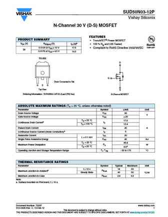
sud50n03.pdf

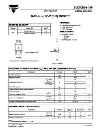
SUD50N03-09P Vishay Siliconix N-Channel 30-V (D-S) MOSFET FEATURES PRODUCT SUMMARY TrenchFET Power MOSFET VDS (V) RDS(on) ( ) ID (A)b Available Optimized for High- or Low-Side 0.0095 at VGS = 10 V 63b RoHS* 100 % Rg Tested 30 COMPLIANT 0.014 at VGS = 4.5 V 52b APPLICATIONS DC/DC Converters Synchronous Rectifiers TO-252 D Drain Connected to T
sqr50n03-06p.pdf
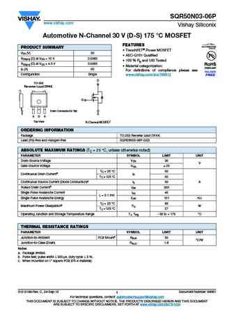
SQR50N03-06P www.vishay.com Vishay Siliconix Automotive N-Channel 30 V (D-S) 175 C MOSFET FEATURES PRODUCT SUMMARY TrenchFET Power MOSFET VDS (V) 30 AEC-Q101 Qualified RDS(on) ( ) at VGS = 10 V 0.0060 100 % Rg and UIS Tested RDS(on) ( ) at VGS = 4.5 V 0.0085 Material categorization ID (A) 50 For definitions of compliance please see Configuration Singl
sud50n03-16p.pdf
SUD50N03-16P New Product Vishay Siliconix N-Channel 30-V (D-S) MOSFET FEATURES PRODUCT SUMMARY D TrenchFETr Power MOSFET D PWM Optimized VDS (V) rDS(on) (W) ID (A)a D 100% Rg Tested 0.016 @ VGS = 10 V 15 APPLICATIONS 30 30 0.024 @ VGS = 4.5 V 12 D High-Side DC/DC - Desktop - Server D D DDR DC/DC Converter TO-252 G Drain Connected to Tab G D S Top View S Ordering Inform
sup50n03-5m1p.pdf

SUP50N03-5m1P Vishay Siliconix N-Channel 30 V (D-S) MOSFET FEATURES PRODUCT SUMMARY Halogen-free According to IEC 61249-2-21 VDS (V) RDS(on) ( ) ID (A) Qg (Typ.) Definition 0.0051 at VGS = 10 V 50d TrenchFET Power MOSFET 30 21.7 0.0063 at VGS = 4.5 V 50d 100 % Rg and UIS Tested Compliant to RoHS Directive 2002/95/EC APPLICATIONS Power Supply - Seco
sqd50n03.pdf
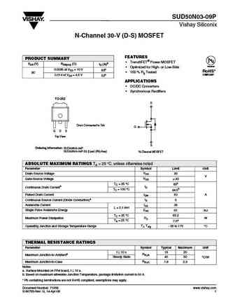
SQD50N03-09 Vishay Siliconix Automotive N-Channel 30 V (D-S) 175 C MOSFET FEATURES PRODUCT SUMMARY Halogen-free According to IEC 61249-2-21 VDS (V) 30 Definition RDS(on) ( ) at VGS = 10 V 0.009 TrenchFET Power MOSFET RDS(on) ( ) at VGS = 4.5 V 0.012 Compliant to RoHS Directive 2002/95/EC ID (A) 50 AEC-Q101 Qualifiedd Configuration Single Find out more
sud50n03-09p.pdf
SUD50N03-09P Vishay Siliconix N-Channel 30-V (D-S) MOSFET FEATURES PRODUCT SUMMARY TrenchFET Power MOSFET VDS (V) RDS(on) ( ) ID (A)b Available Optimized for High- or Low-Side 0.0095 at VGS = 10 V 63b RoHS* 100 % Rg Tested 30 COMPLIANT 0.014 at VGS = 4.5 V 52b APPLICATIONS DC/DC Converters Synchronous Rectifiers TO-252 D Drain Connected to T
sud50n03-10.pdf
SUD50N03-10 Siliconix N-Channel 30-V (D-S), 175_C MOSFET Product Summary VDS (V) rDS(on) (W) ID (A) 0.010 @ VGS = 10 V "15 30 30 0.019 @ VGS = 4.5 V "12 D TO-252 G Drain Connected to Tab G D S Top View Order Number S SUD50N03-10 N-Channel MOSFET Absolute Maximum Ratings (TA = 25_C Unless Otherwise Noted) Parameter Symbol Limit Unit Drain-Source Voltage VDS 30 V V Gate-
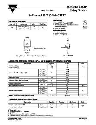
sud50n03-12p.pdf
SUD50N03-12P Vishay Siliconix N-Channel 30 V (D-S) MOSFET FEATURES PRODUCT SUMMARY TrenchFET Power MOSFET VDS (V) RDS(on) ( ) ID (A)a 100 % Rg and UIS Tested 0.0120 at VGS = 10 V 17.5 Compliant to RoHS Directive 2002/95/EC 30 0.0175 at VGS = 4.5 V 14.5 TO-252 D G Drain Connected to Tab G D S Top View S Ordering Information SUD50N03-12P-E3 (Lead (PB) fr
sqd50n03-09.pdf
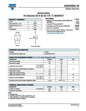
SQD50N03-09 www.vishay.com Vishay Siliconix Automotive N-Channel 30 V (D-S) 175 C MOSFET FEATURES PRODUCT SUMMARY Halogen-free According to IEC 61249-2-21 VDS (V) 30 Definition RDS(on) ( ) at VGS = 10 V 0.009 TrenchFET Power MOSFET RDS(on) ( ) at VGS = 4.5 V 0.012 100 % Rg and UIS Tested ID (A) 50 Compliant to RoHS Directive 2002/95/EC Configuration Single
sud50n03-06ap.pdf
SUD50N03-06AP New Product Vishay Siliconix N-Channel 30-V (D-S) MOSFET FEATURES PRODUCT SUMMARY D TrenchFETr Power MOSFET VDS (V) rDS(on) (W) ID (A)a, e Qg (Typ) D Optimized for Low Side Synchronous Rectifier Operation 0.0057 @ VGS = 10 V 90 RoHS 30 30 30 30 COMPLIANT D 100% Rg Tested 0.0078 @ VGS = 4.5 V 77 APPLICATIONS D DC/DC Converters D Synchronous Rectifiers TO-252 D
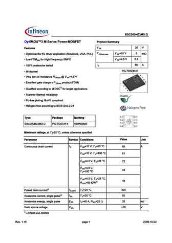
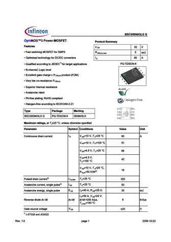
bsc050n03ms.pdf
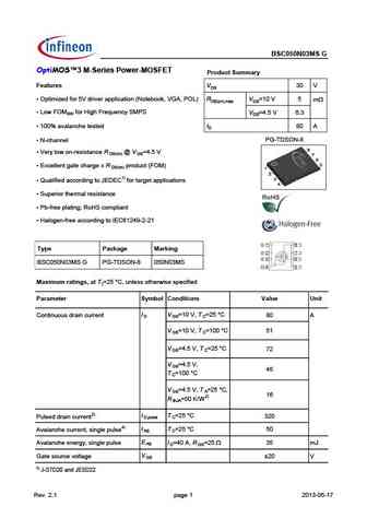
BSC050N03MS G OptiMOS 3 M-Series Power-MOSFET Product Summary Features VDS 30 V Optimized for 5V driver application (Notebook, VGA, POL) RDS(on),max VGS=10 V 5 mW Low FOMSW for High Frequency SMPS VGS=4.5 V 6.3 100% avalanche tested ID 80 A PG-TDSON-8 N-channel Very low on-resistance R @ V =4.5 V DS(on) GS Excellent gate charge x R product (FOM) DS
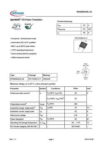
ipd50n03s2-07.pdf
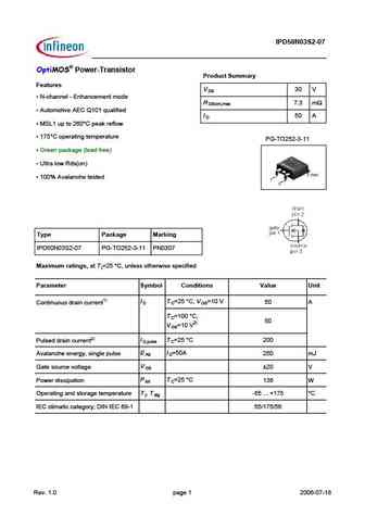
IPD50N03S2-07 OptiMOS Power-Transistor Product Summary Features V 30 V DS N-channel - Enhancement mode R 7.3 m DS(on),max Automotive AEC Q101 qualified I 50 A D MSL1 up to 260 C peak reflow 175 C operating temperature PG-TO252-3-11 Green package (lead free) Ultra low Rds(on) 100% Avalanche tested Type Package Marking IPD50N03S2-07 PG-TO252-
bsz050n03ms.pdf

BSZ050N03MS G OptiMOS 3 M-Series Power-MOSFET Product Summary Features V 30 V DS Optimized for 5V driver application (Notebook, VGA, POL) R V =10 V 4.5 m DS(on),max GS Low FOMSW for High Frequency SMPS V =4.5 V 5.7 GS 100% avalanche tested I 40 A D PG-TSDSON-8 N-channel Very low on-resistance R @ V =4.5 V DS(on) GS Excellent gate charge x R product
ipd50n03s2l-06.pdf
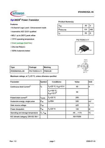
IPD50N03S2L-06 OptiMOS Power-Transistor Product Summary Features V 30 V DS N-channel Logic Level - Enhancement mode R 6.4 m DS(on),max Automotive AEC Q101 qualified I 50 A D MSL1 up to 260 C peak reflow 175 C operating temperature PG-TO252-3-11 Green package (lead free) Ultra low Rds(on) 100% Avalanche tested Type Package Marking IPD50N03S2
bsc150n03ld.pdf
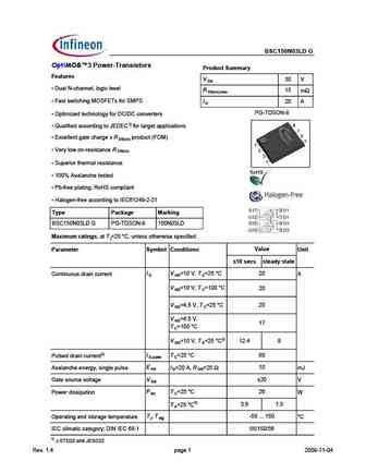
BSC150N03LD G OptiMOS 3 Power-Transistors Product Summary Features V 30 V DS Dual N-channel, logic level R 15 m DS(on),max Fast switching MOSFETs for SMPS I 20 A D PG-TDSON-8 Optimized technology for DC/DC converters Qualified according to JEDEC1) for target applications Excellent gate charge x R product (FOM) DS(on) Very low on-resistance R DS(on
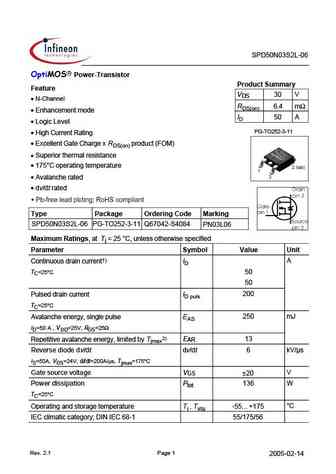
spd50n03s2l-06.pdf
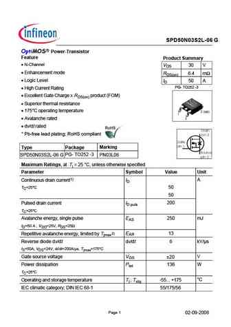
SPD50N03S2L-06 OptiMOS Power-Transistor Feature Product Summary N-Channel VDS 30 V Enhancement mode RDS(on) 6.4 m Logic Level ID 50 A P - TO252 -3 High Current Rating Excellent Gate Charge x RDS(on) product (FOM) Superior thermal resistance 175 C operating temperature Avalanche rated dv/dt rated Ug2kwjj qjfi uqfynsl@ W tMX htruqnfsy
bsc050n03msg5.pdf
% ! % D %0 S 07DK >AI A@ D7E;EF3@57 0 D n) G S J57>>7@F 93F7 5 3D97 J BDA6G5F !* ( D n) 1) S , G3>;8;76 355AD6;@9 FA % 8AD F3D97F 3BB>;53F;A@E S .GB7D;AD F 7D?3> D7
spd50n03s2l-06 spd50n03s2l-06t.pdf
SPD50N03S2L-06 OptiMOS Power-Transistor Product Summary Feature VDS 30 V N-Channel RDS(on) 6.4 m Enhancement mode ID 50 A Logic Level PG-TO252-3-11 High Current Rating Excellent Gate Charge x RDS(on) product (FOM) Superior thermal resistance 175 C operating temperature Avalanche rated dv/dt rated Type Package Ordering Code Marking SP
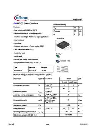
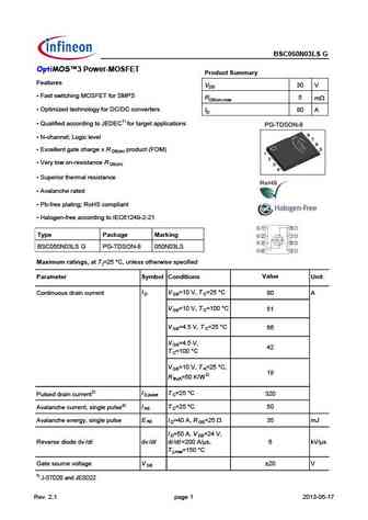
bsc050n03ls.pdf

BSC050N03LS G OptiMOS 3 Power-MOSFET Product Summary Features VDS 30 V Fast switching MOSFET for SMPS RDS(on),max 5 mW Optimized technology for DC/DC converters ID 80 A Qualified according to JEDEC1) for target applications PG-TDSON-8 N-channel; Logic level Excellent gate charge x R product (FOM) DS(on) Very low on-resistance R DS(on) Superio
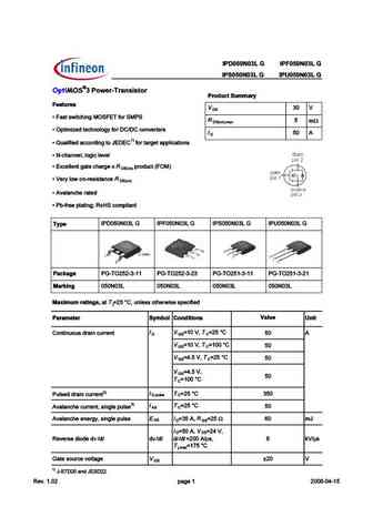
ipf050n03lg.pdf
Type IPD050N03L G IPF050N03L G IPS050N03L G IPU050N03L G OptiMOS 3 Power-Transistor Product Summary Features V 30 V DS Fast switching MOSFET for SMPS R 5 m DS(on),max Optimized technology for DC/DC converters I 50 A D Qualified according to JEDEC1) for target applications N-channel, logic level Excellent gate charge x R product (FOM) DS(on) Very low
ipd050n03lg ipf050n03lg ips050n03lg ipu050n03lg ipd050n03l ips050n03l.pdf
Type IPD050N03L G IPF050N03L G IPS050N03L G IPU050N03L G OptiMOS 3 Power-Transistor Product Summary Features VDS 30 V Fast switching MOSFET for SMPS RDS(on),max 5 mW Optimized technology for DC/DC converters ID 50 A Qualified according to JEDEC1) for target applications N-channel, logic level Excellent gate charge x R product (FOM) DS(on) Very low on
bsf050n03lq3g.pdf
n-Channel Power MOSFET OptiMOS BSF050N03LQ3 G Data Sheet 2.2, 2009-05-11 Final Industrial & Multimarket OptiMOS Power-MOSFET BSF050N03LQ3 G 1 Description OptiMOS 30V products are class leading power MOSFETs for highest power density and energy efficient solutions. Ultra low gate- and output charges together with lowest on state resistance in small footprint packages make
bsc150n03ldg.pdf

BSC150N03LD G OptiMOS 3 Power-Transistors Product Summary Features V 30 V DS Dual N-channel, logic level R 15 m DS(on),max Fast switching MOSFETs for SMPS I 20 A D PG-TDSON-8 Optimized technology for DC/DC converters Qualified according to JEDEC1) for target applications Excellent gate charge x R product (FOM) DS(on) Very low on-resistance R DS(on
spd50n03s2-07 .pdf

SPD50N03S2-07 G OptiMOS Power-Transistor Product Summary Feature VDS 30 V N-Channel RDS(on) 7.3 m Enhancement mode ID 50 A Excellent Gate Charge x RDS(on) product (FOM) P -TO252-3 Superior thermal resistance 175 C operating temperature Avalanche rated dv/dt rated Ug2kwjj qjfi uqfynsl@ W tMX htruqnfsy Type Package Marking SPD50N03S2-07 L PN0307
ipd050n03l ipf050n03l ips050n03l ipu050n03l.pdf

Type IPD050N03L G IPF050N03L G IPS050N03L G IPU050N03L G OptiMOS 3 Power-Transistor Product Summary Features V 30 V DS Fast switching MOSFET for SMPS R 5 m DS(on),max Optimized technology for DC/DC converters I 50 A D Qualified according to JEDEC1) for target applications N-channel, logic level Excellent gate charge x R product (FOM) DS(on) Very low
bsc050n03ls .pdf
& " & E $;B1= !#& ' $=;0@/? &@99-=D Features D Q 2CD CG D49 ?8 ') - . 7@B -'*- m D n) m x Q ) AD > J65 D649?@=@8I 7@B 4@?F6BD6BC D 1) Q + E2= 7 65 244@B5 ?8 D@ $ 7@B D2B86D 2AA= 42D @?C G D ON Q ( 492??6= &@8 4 =6F6= Q H46==6?D 82D6 492B86 H AB@5E4D ) ' D n) Q /6BI =@G @? B6C CD2?46 D n) Q -EA6B @B D96B>2= B6C CD2?46 Q F2=2?496 B2D65 Q *3 7B66 A=2D ?8 , @"- 4@>
bsc050n03lsg.pdf
BSC050N03LS G OptiMOS 3 Power-MOSFET Product Summary Features VDS 30 V Fast switching MOSFET for SMPS RDS(on),max 5 mW Optimized technology for DC/DC converters ID 80 A Qualified according to JEDEC1) for target applications PG-TDSON-8 N-channel; Logic level Excellent gate charge x R product (FOM) DS(on) Very low on-resistance R DS(on) Superio
ipd050n03lg.pdf
pe % # ! % # ! %' # ! %) # ! % (>.;?6?@ %>E Features D R 3DE DH;E5 ;@9 ') - . 8AC -'*- m D n) m x R ) BE;?;K76 E75 @A>A9J 8AC 5A@G7CE7CD D 1) R + F3>;8;76 355AC6;@9 EA $ 8AC E3C97E 3BB>;53E;A@D R ( 5 3@@7> >A9;5 >7G7> R I57>>7@E 93E7 5 3C97 I BCA6F5E ) ' D n) R 07CJ >AH A@ C7D;DE3@57 D n) R G3>3@5 7 C3E76 R *4 8C77 B>3E;@9 , A"- 5A?B>;3@E Type
ipd050n03lg2.pdf

pe % # ! % # ! %' # ! %) # ! % (>.;?6?@ %>E Features D R 3DE DH;E5 ;@9 ') - . 8AC -'*- m D n) m x R ) BE;?;K76 E75 @A>A9J 8AC 5A@G7CE7CD D 1) R + F3>;8;76 355AC6;@9 EA $ 8AC E3C97E 3BB>;53E;A@D R ( 5 3@@7> >A9;5 >7G7> R I57>>7@E 93E7 5 3C97 I BCA6F5E ) ' D n) R 07CJ >AH A@ C7D;DE3@57 D n) R G3>3@5 7 C3E76 R *4 8C77 B>3E;@9 , A"- 5A?B>;3@E Type
bsz050n03lsg.pdf

BSZ050N03LS G OptiMOS 3 Power-MOSFET Product Summary Features V 30 V DS Fast switching MOSFET for SMPS R 5 m DS(on),max Optimized technology for DC/DC converters I 40 A D Qualified according to JEDEC1) for target applications PG-TSDSON-8 N-channel; Logic level Excellent gate charge x R product (FOM) DS(on) Very low on-resistance R DS(on) Superio
bsz050n03msg.pdf
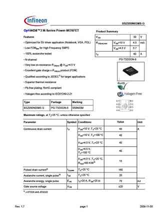
BSZ050N03MS G OptiMOS 3 M-Series Power-MOSFET Product Summary Features V 30 V DS Optimized for 5V driver application (Notebook, VGA, POL) R V =10 V 4.5 m DS(on),max GS Low FOMSW for High Frequency SMPS V =4.5 V 5.7 GS 100% avalanche tested I 40 A D PG-TSDSON-8 N-channel Very low on-resistance R @ V =4.5 V DS(on) GS Excellent gate charge x R product
spd50n03s2-07.pdf
SPD50N03S2-07 G OptiMOS Power-Transistor Product Summary Feature VDS 30 V N-Channel RDS(on) 7.3 m Enhancement mode ID 50 A Excellent Gate Charge x RDS(on) product (FOM) P -TO252-3 Superior thermal resistance 175 C operating temperature Avalanche rated dv/dt rated Ug2kwjj qjfi uqfynsl@ W tMX htruqnfsy Type Package Marking SPD50N03S2-07 L PN0307
bsz050n03ls.pdf
BSZ050N03LS G OptiMOS 3 Power-MOSFET Product Summary Features V 30 V DS Fast switching MOSFET for SMPS R 5 m DS(on),max Optimized technology for DC/DC converters I 40 A D Qualified according to JEDEC1) for target applications PG-TSDSON-8 N-channel; Logic level Excellent gate charge x R product (FOM) DS(on) Very low on-resistance R DS(on) Superio
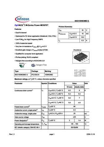
bso150n03mdg.pdf
BSO150N03MD G OptiMOS 3 M-Series Power-MOSFET Product Summary Features V 30 V DS Dual N-channel R V =10 V 15 m DS(on),max GS Optimized for 5V driver application (Notebook, VGA, POL) V =4.5 V 18.2 GS Low FOMSW for High Frequency SMPS I 9.3 A D 100% Avalanche tested Very low on-resistance R @ V =4.5 V DS(on) GS Excellent gate charge x R product (FOM
bso150n03 rev1.7 g.pdf
BSO150N03 "9@/; %;+877+;B Features V DS Q 2CD CG D49 ?8 ') - . 7@B -'*- m DS(on) max Q ) AD > J65 D649?@=@8I 7@B ?@D63@@2= B6C CD2?46 Q F2=2?496 B2D
ipd50n03s4l-06 ipd50n03s4l-06 ds 1 1.pdf
IPD50N03S4L-06 OptiMOS -T2 Power-Transistor Product Summary V 30 V DS R 5.5 mW DS(on),max I 50 A D PG-TO252-3-11 N-channel - Enhancement mode Automotive AEC Q101 qualified MSL1 up to 260 C peak reflow 175 C operating temperature Green product (RoHS compliant) 100% Avalanche tested Type Package Marking IPD50N03S4L-06 PG-TO252-3-11 4N03L06 Maximum rat
bso150n03md.pdf
%" ! %0;53F;A@ ) AF74AA= 0" +* ' 0 1 G S 'AI !* ( 8AD #;9 !D7CG7@5K .( +. D S H3>3@5 7 F7EF76 S 07DK >AI A@ D7E;EF3@57 0 D n) G S J57>>7@F 93F7 5 3D97 J BDA6G5F !* ( G D O D n) S , G3>;8;76 8AD 5A@EG?7D >7H7> 3BB>;53F;A@ S +4 8D77 B>3F;@9 - A#. 5A?B>
mcg50n03.pdf
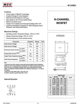
MCG50N03 Features Trench Power LV MOSFET Technology Excellent Package for Heat Dissipation High Density Cell Design for Low RDS(on) Epoxy Meets UL 94 V-0 Flammability Rating N-CHANNEL Moisture Sensitivity Level 1 MOSFET Halogen Free Available Upon Request By Adding Suffix "-HF" Lead Free Finish/RoHS Compliant ("P" Suffix Designates RoHS Compliant. See Order
ntd50n03r-d ntd50n03r.pdf
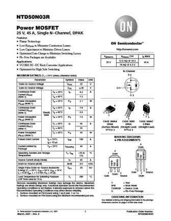
NTD50N03R Power MOSFET 25 V, 45 A, Single N-Channel, DPAK Features Planar Technology Low RDS(on) to Minimize Conduction Losses http //onsemi.com Low Capacitance to Minimize Driver Losses Optimized Gate Charge to Minimize Switching Losses V(BR)DSS RDS(on) TYP ID MAX Pb-Free Packages are Available 12.5 mW @ 10 V Applications 25 V 45 A 19 mW @ 4.5 V VCORE DC-
fdd050n03b.pdf

Is Now Part of To learn more about ON Semiconductor, please visit our website at www.onsemi.com Please note As part of the Fairchild Semiconductor integration, some of the Fairchild orderable part numbers will need to change in order to meet ON Semiconductor s system requirements. Since the ON Semiconductor product management systems do not have the ability to manage part nomenclatur
utt150n03.pdf
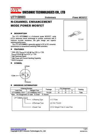
UNISONIC TECHNOLOGIES CO., LTD UTT150N03 Preliminary Power MOSFET N-CHANNEL ENHANCEMENT MODE POWER MOSFET DESCRIPTION The UTC UTT150N03 is a N-channel power MOSFET, using UTC s advanced trench technology to provide customers with a minimum on-state resistance, low gate charge and superior switching performance. The UTC UTT150N03 is generally applied in DC to DC convertor,
ut50n03.pdf
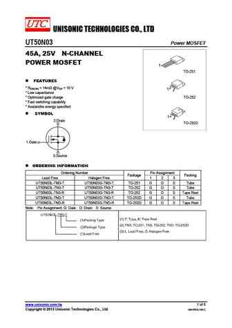
UNISONIC TECHNOLOGIES CO., LTD UT50N03 Power MOSFET 45A, 25V N-CHANNEL POWER MOSFET 1 TO-251 FEATURES * RDS(ON)
gfd50n03a.pdf
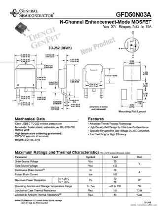
GFD50N03A N-Channel Enhancement-Mode MOSFET V 30V R 7 I 78A DS DS(ON) m D D TO-252 (DPAK) G 0.265 (6.73) 0.094 (2.39) 0.255 (6.48) 0.087 (2.21) S 0.214 (5.44) 0.023 (0.58) 0.206 (5.23) 0.018 (0.46) 0.190 www.DataSheet4U.com (4.826) D 0.050 (1.27) 0.035 (0.89) 0.165 (4.191) 0.170 (4.32) min. 0.245 (6.22) 0.235 (5.97) 0.410 (10.41) 0.060 (1.52) 0.380 (9.65) 0.100 0.0
cjac150n03.pdf
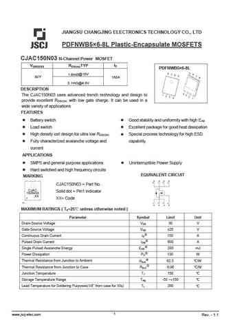
JIANGSU CHANGJING ELECTRONICS TECHNOLOGY CO., LTD PDFN 5 6-8L Plastic-Encapsulate MOSFETS CJAC150N03 N-Channel Power MOSFET ID V(BR)DSS RDS(on)TYP PDFN 5 6-8L 1.6m @10V 30 V 150A 2.1m @4.5V DESCRIPTION 15 FEATURES
h50n03j.pdf
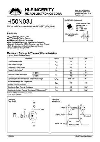
Spec. No. MOS200514 HI-SINCERITY Issued Date 2005.01.01 Revised Date 2005.10.14 MICROELECTRONICS CORP. Page No. 1/5 H50N03J Pin Assignment H50N03J Tab 3-Lead Plastic TO-252 Package Code J N-Channel Enhancement-Mode MOSFET (25V, 50A) Pin 1 Gate 3 Pin 2 & Tab Drain 2 1 Pin 3 Source D Features Internal Schematic Diagram RDS(on)=6m @VGS=10V, ID=30A G RDS
am50n03-12i.pdf
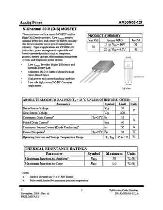
Analog Power AM50N03-12I N-Channel 30-V (D-S) MOSFET These miniature surface mount MOSFETs utilize PRODUCT SUMMARY High Cell Density process. Low rDS(on) assures VDS (V) rDS(on) m( ) ID (A) minimal power loss and conserves energy, making this device ideal for use in power management 13 @ VGS = 10V 51 circuitry. Typical applications are PWMDC-DC 30 20 @ VGS = 4.5V 41 converters,
am50n03-12d.pdf
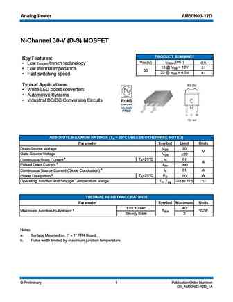
Analog Power AM50N03-12D N-Channel 30-V (D-S) MOSFET PRODUCT SUMMARY Key Features rDS(on) (m ) VDS (V) ID(A) Low r trench technology DS(on) 13 @ VGS = 10V 51 Low thermal impedance 30 20 @ VGS = 4.5V 41 Fast switching speed Typical Applications White LED boost converters Automotive Systems Industrial DC/DC Conversion Circuits ABSOLUTE MAXIMUM
g50n03k.pdf
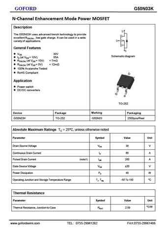
GOFORD G50N03K N-Channel Enhancement Mode Power MOSFET Description The G50N03K uses advanced trench technology to provide excellent RDS(ON) , low gate charge. It can be used in a wide variety of applications. General Features VDS 30V Schematic diagram ID (at VGS = 10V) 65A RDS(ON) (at VGS = 10V)
g50n03a.pdf
GOFORD G50N03A DESCRIPTION The G50N03A uses advanced trench technology And design to provide excellent RDS (ON ) with Low gate charge . It can be used in a wide TO-252 Vanety of applications . GENERAL FEATURES VDSS RDS(ON) RDS(ON) ID @ 4.5V (Typ) @ 10V (Typ) 30V 10m 6.2 m 50 A High density cell design for ultra low Rdson Fully characterized Avalanche voltage
p50n03ltg.pdf
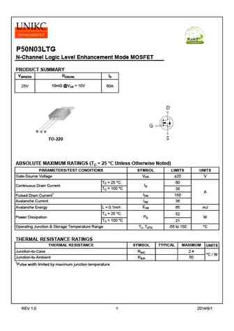
P50N03LTG N-Channel Logic Level Enhancement Mode MOSFET PRODUCT SUMMARY V(BR)DSS RDS(ON) ID 10m @VGS = 10V 25V 60A TO-220 ABSOLUTE MAXIMUM RATINGS (TC = 25 C Unless Otherwise Noted) PARAMETERS/TEST CONDITIONS SYMBOL LIMITS UNITS VGS Gate-Source Voltage 20 V TC = 25 C 60 ID Continuous Drain Current TC = 100 C 38 A IDM 150 Pulsed Drain Current1 IAS Avalanche
brd50n03.pdf
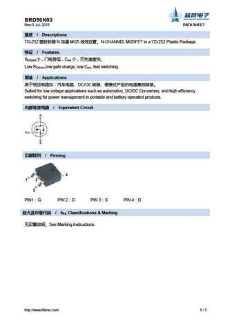
BRD50N03 Rev.G Jul.-2018 DATA SHEET / Descriptions TO-252 N MOS N-CHANNEL MOSFET in a TO-252 Plastic Package. / Features R C DS(on) rss Low RDS(on),low gate charge, low Crss, fast switching. / Applications DC/DC
brcs050n03zc.pdf
BRCS050N03ZC Rev.B Jul.-2022 DATA SHEET / Descriptions PDFN5 6 N N-Channel MOSFET in a PDFN5 6 Plastic Package. / Features Low RDS(ON) to minimize conductive loss;low Gate Charge for fast switching;Low Thermal resistance;HF
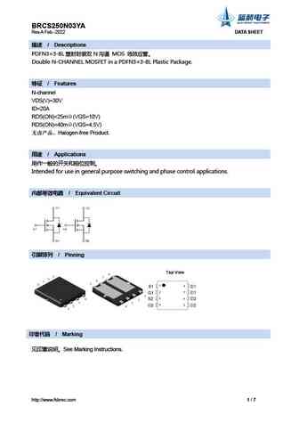
brcs250n03dmf.pdf
BRCS250N03DMF Rev.A Nov.-2021 DATA SHEET / Descriptions SOT23-6 N MOS Dual N-Channel MOSFET in a SOT23-6 Plastic Package. / Features Super high dense cell design for low R ,Rugged and reliable,HF product. DS(ON) / Applications
br50n03.pdf
BR50N03 Rev.B Jul.-2018 DATA SHEET / Descriptions TO-220 N MOS N-CHANNEL MOSFET in a TO-220 Plastic Package. / Features , , Low gate charge, low crss, fast switching. / Applications DC/DC .S
bri50n03.pdf
BRI50N03(BRCS50N03I) Rev.C Feb.-2015 DATA SHEET / Descriptions TO-251 N MOS N-CHANNEL MOSFET in a TO-251 Plastic Package. / Features R C DS(on) rss Low RDS(on),low gate charge, low Crss, fast speed switching. / Applications DC/DC
cs150n03 a8.pdf
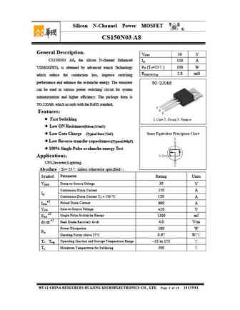
Silicon N-Channel Power MOSFET R CS150N03 A8 General Description VDSS 30 V CS150N03 A8, the silicon N-channel Enhanced ID 150 A PD (TC=25 ) 100 W VDMOSFETs, is obtained by advanced trench Technology RDS(ON)Typ 2.8 m which reduce the conduction loss, improve switching performance and enhance the avalanche energy. The transistor can be used in various power sw
ftk50n03d.pdf
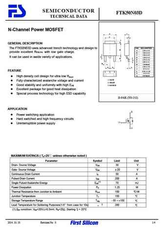
SEMICONDUCTOR FTK50N03D TECHNICAL DATA N-Channel Power MOSFET A I C J GENERAL DESCRIPTION The FTK50N03D uses advanced trench technology and design to DIM MILLIMETERS A 6 50 0 2 provide excellent RDS(ON) with low gate charge. B 5 60 0 2 C 5 20 0 2 It can be used in awide variety of applications. D 1 50 0 2 E 2 70 0 2 F 2 30 0 1 H H 1 00 MAX I 2 30 0
dhp150n03.pdf
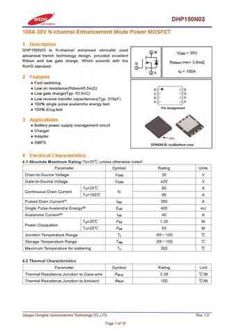
DHP150N03 100A 30V N-channel Enhancement Mode Power MOSFET 1 Description DHP150N03 Is N-channel enhanced vdmosfet used 2 D V = 35V DSS advanced trench technology design, provided excellent Rdson and low gate charge. Which accords with the R = 3.6m DS(on) (TYP) G RoHS standard. 1 I = 100A D 3 S 2 Features Fast switching Low on resistance(Rdson 5.5m ) Low gate
dhb50n03 dhd50n03.pdf
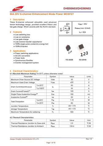
DHB50N03/DHD50N03 50A 30V N-channel Enhancement Mode Power MOSFET 1 Description These N-channel enhanced vdmosfets used advanced 2 D V = 30V DSS trench technology design, provided excellent Rdson and low gate charge. Which accords with the RoHS standard. R = 6.0m DS(on) (TYP) G 1 2 Features I = 50A 3 S D Low switching loss Low on resistance Low gate charge Lo
ndt50n03.pdf
SMD Type MOSFET N-Channel MOSFET NDT50N03 TO-252 Unit mm +0.15 6.50-0.15 +0.1 2.30 -0.1 Features +0.2 5.30-0.2 +0.8 0.50 -0.7 VDS (V) = 30V ID = 90 A (VGS = 10V) D RDS(ON) 5.7m (VGS = 10V) 0.127 +0.1 0.80-0.1 RDS(ON) 7.8m (VGS = 4.5V) max G + 0.1 1Gate 2.3 0.60- 0.1 +0.15 4.60 -0.15 2Drain 3Source S Absolute Maximum Ratings
msd50n03.pdf
Bruckewell Technology Corp., Ltd. MSD50N03 N-Channel Logic Level Enhancement Mode Power MOSFET FEATURES VDS=30V, ID=50A, RDS(ON)=9m Low Gate Charge Repetitive Avalanche Rated Simple Drive Requirement Fast Switching Characteristic RoHS compliant package Absolute Maximum Ratings (Tc=25 C unless otherwise noted) Parameter Symbol Value Unit Drai
pjs50n03.pdf
PJS50N03 30V N-CHANNEL ENHANCEMENT MODE MOSFET 30 Volts 2.9 Amperes VOLTAGE CURRENT FEATURES RDS(ON), VGS@10V,ID@3.1A
fhd150n03b.pdf
N N-CHANNEL MOSFET FHD150N03B MAIN CHARACTERISTICS FEATURES ID 150 A Low gate charge VDSS 30 V Crss ( 405pF) Low Crss (typical 405pF ) Rdson-typ @Vgs=10V 2.2m Fast switching Rdson-typ @Vgs=4.5V 2.8m 100% 100% avalanche tested Qg-typ
fhp150n03a fhs150n03a fhd150n03a.pdf
N N-CHANNEL MOSFET FHP150N03A/FHS150N03A/FHD150N03A MAIN CHARACTERISTICS FEATURES ID 150 A Low gate charge VDSS 30V Crss ( 314pF) Low Crss (typical 314pF ) Rdson-typ @Vgs=10V 2.5m Fast switching Rdson-typ @Vgs=4.5V 3.2m 100% 100% avalanc
fhp150n03c.pdf
N N-CHANNEL MOSFET FHP150N03C MAIN CHARACTERISTICS FEATURES ID 150 A Low gate charge VDSS 26 V Crss ( 405pF) Low Crss (typical 405pF ) Rdson-typ @Vgs=10V 2.2m Fast switching Rdson-typ @Vgs=4.5V 2.8m 100% 100% avalanche tested Qg-typ
kia50n03bd.pdf
50A30V N-CHANNELMOSFET KIA50N03B KIA KIA KIA SEMICONDUCTORS SEMICONDUCTORS SEMICONDUCTORS 1. Features Advanced trenchprocess technology High density cell design for ultra lowon-resistance Fully characterized avalanche voltage and current 2. Features 50A, 30V, R (on) typ. =6.5m (typ.)@V =10 V DS GS Lowgate charge LowCrss Fast switching Improveddv/dt capability 3. Pinc
kia50n03.pdf
50 Amps, 30 Volts N-CHANNEL MOSFET 50N03 KIA KIA KIA SEMICONDUCTORS SEMICONDUCTORS SEMICONDUCTORS 1.Features Advanced trench process technology High density cell design for ultra low on-resistance Fully characterized avalanche voltage and current 2.Applications VDSS=30V,RDS(on)=6.5m ,ID=50A Vds=30V RDS(ON)=6.5m (Max.),VGS@10V,Ids@30A RDS(
sl150n03q.pdf
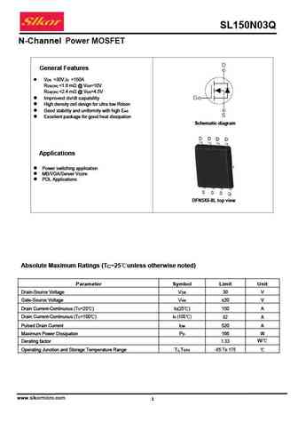
SL150N03Q N-Channel Power MOSFET General Features VDS =30V,ID =150A RDS(ON)
wmq050n03lg4.pdf
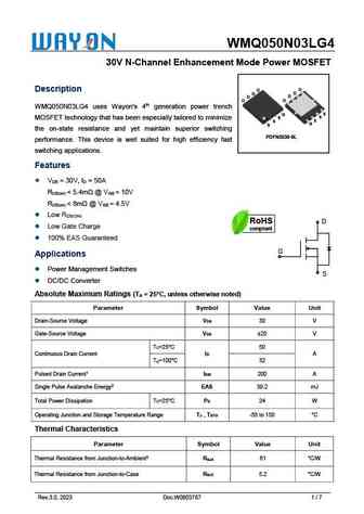
WMQ050N03LG4 30V N-Channel Enhancement Mode Power MOSFET D Description D D D D D D D WMQ050N03LG4 uses Wayon's 4th generation power trench S G S MOSFET technology that has been especially tailored to minimize S S S G S the on-state resistance and yet maintain superior switching PDFN3030-8L performance. This device is well suited for high efficiency fast switching app
wmb050n03lg4.pdf
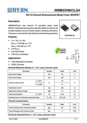
WMB050N03LG4 30V N-Channel Enhancement Mode Power MOSFET Description D D D D WMB050N03LG4 uses Wayon's 4th generation power trench D D D D MOSFET technology that has been especially tailored to minimize the G ss s ss on-state resistance and yet maintain superior switching performance. G s This device is well suited for high efficiency fast switching applications. PDFN506
wmr050n03lg4.pdf
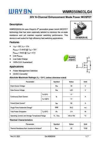
WMR050N03LG4 30V N-Channel Enhancement Mode Power MOSFET G D Pin1 D S Description D S D S D D D WMR050N03LG4 uses Wayon's 4th generation power trench MOSFET technology that has been especially tailored to minimize the on-state G D resistance and yet maintain superior switching performance. This D DFN2020-6L device is well suited for high efficiency fast switching appli
wmb150n03ts.pdf
WMB150N03TS 30V N-Channel Enhancement Mode Power MOSFET Description D D D D D D D D WMB150N03TS uses advanced power trench technology that has G been especially tailored to minimize the on-state resistance and yet ss s ss G s maintain superior switching performance. Features PDFN5060-8L V = 30V, I = 150A DS D R
cs150n03a8.pdf
Huajing Discrete Devices R Silicon N-Channel Power MOSFET CS150N03A8 General Description VDSS 30 V CS150N03A8, the silicon N-channel Enhanced ID 150 A PD (TC=25 ) 100 W VDMOSFETs, is obtained by advanced trench Technology RDS(ON)Typ 2.8 m which reduce the conduction loss, improve switching performance and enhance the avalanche energy. The transistor can b
emf50n03js.pdf
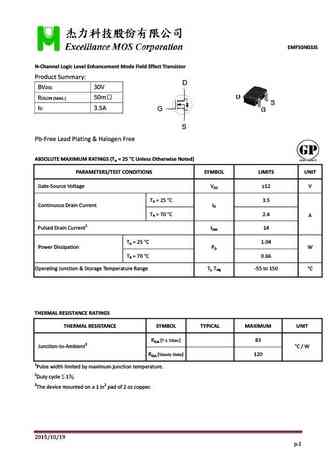
EMF50N03JS N Channel Logic Level Enhancement Mode Field Effect Transistor Product Summary D BVDSS 30V RDSON (MAX.) 50m ID 3.5A G S Pb Free Lead Plating & Halogen Free ABSOLUTE MAXIMUM RATINGS (TA = 25 C Unless Otherwise Noted) PARAMETERS/TEST CONDITIONS SYMBOL LIMITS UNIT Gate Source Voltage VGS 12 V TA = 25 C 3
hsu150n03.pdf
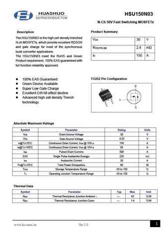
HSU150N03 N-Ch 30V Fast Switching MOSFETs Product Summary Description The HSU150N03 is the high cell density trenched VDS 30 V N-ch MOSFETs, which provide excellent RDSON and gate charge for most of the synchronous RDS(ON),typ 2.4 m buck converter applications. ID 150 A The HSU150N03 meet the RoHS and Green Product requirement, 100% EAS guaranteed with full function
jmtk50n03a.pdf
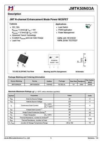
JMTK50N03A Description JMT N-channel Enhancement Mode Power MOSFET Features Applications 30V, 50A Load Switch RDS(ON)
skq50n03bd.pdf
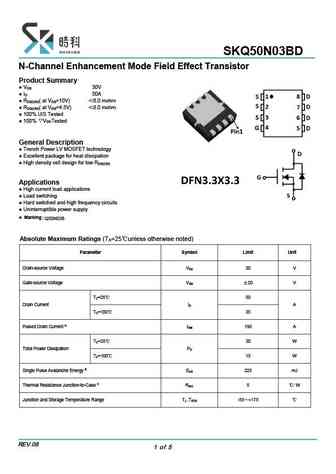
SKQ50N03BD N-Channel Enhancement Mode Field Effect Transistor Product Summary V 30V DS I 50A D R ( at V =10V) 6.0 mohm DS(ON) GS R ( at V =4.5V) 8.0 mohm DS(ON) GS 100% UIS Tested 100% VDS Tested General Description Trench Power LV MOSFET technology Excellent package for heat dissipation High density cell design for low R
hts050n03.pdf
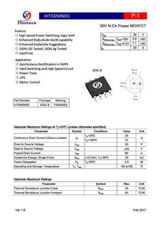
HTS050N03 P-1 30V N-Ch Power MOSFET Feature 30 V VDS High Speed Power Switching, logic level 3.9 RDS(on),typ VGS=10V m Enhanced Body diode dv/dt capability 7.1 RDS(on),typ VGS=4.5V m Enhanced Avalanche Ruggedness 20 A ID 100% UIS Tested, 100% Rg Tested Lead Free Application Synchronous Rectification in SMPS Hard Switching and High Speed Circui
htj350n03.pdf
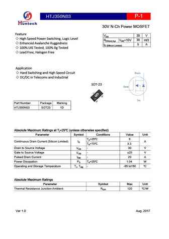
HTJ350N03 P-1 30V N-Ch Power MOSFET Feature 30 V VDS High Speed Power Switching, Logic Level 30 RDS(on),typ VGS=10V m Enhanced Avalanche Ruggedness 5 A ID (Sillicon Limited) 100% UIS Tested, 100% Rg Tested Lead Free, Halogen Free Application Hard Switching and High Speed Circuit Drain DC/DC in Telecoms and Inductrial SOT-23 Gate Src Part Number Pack
hto350n03.pdf
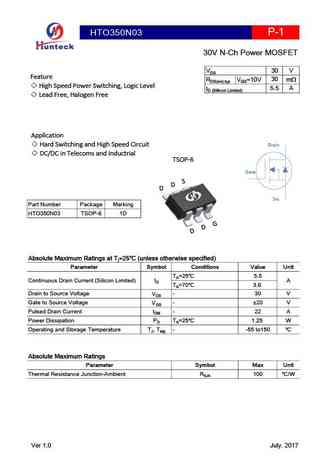
HTO350N03 P-1 30V N-Ch Power MOSFET 30 V VDS Feature 30 RDS(on),typ VGS=10V m High Speed Power Switching, Logic Level 5.5 A ID (Sillicon Limited) Lead Free, Halogen Free Application Hard Switching and High Speed Circuit Drain DC/DC in Telecoms and Inductrial TSOP-6 Gate Src Part Number Package Marking HTO350N03 TSOP-6 1D Absolute Maximum Ratings at Tj=25
vbzm50n03.pdf
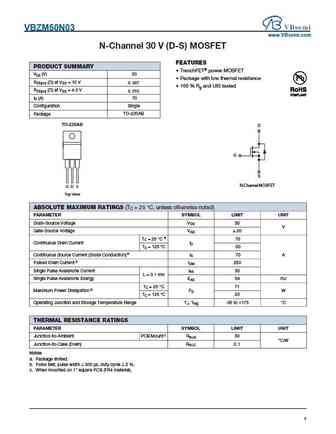
VBZM50N03 www.VBsemi.com N-Channel 30 V (D-S) MOSFET FEATURES PRODUCT SUMMARY TrenchFET power MOSFET VDS (V) 30 Package with low thermal resistance RDS(on) ( ) at VGS = 10 V 0.007 100 % Rg and UIS tested RDS(on) ( ) at VGS = 4.5 V 0.010 ID (A) 70 Configuration Single TO-220AB Package TO-220AB D G S N-Channel MOSFET G D S Top View ABSOLUTE MAXIMUM RATIN
vbzqa50n03.pdf
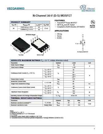
VBZQA50N03 www.VBsemi.com N-Channel 30-V (D-S) MOSFET FEATURES PRODUCT SUMMARY TrenchFET Power MOSFET VDS (V) RDS(on) ( ) ID (A)a, e Qg (Typ) 100 % Rg and UIS Tested Compliant to RoHS Directive 2011/65/EU 0.007 at VGS = 10 V 80 30 31 nC 0.009 at VGS = 4.5 V 60 APPLICATIONS OR-ing DFN5X6 Single D D Server D 8 DC/DC D 7 D 6 5 G 1 2 S S 3 S
vbzfb50n03.pdf
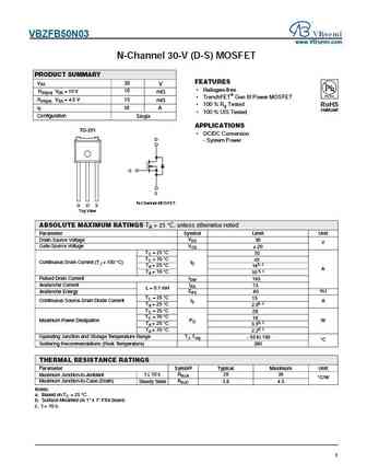
VBZFB50N03 www.VBsemi.com N-Channel 30-V (D-S) MOSFET PRODUCT SUMMARY FEATURES VDS 30 V Halogen-free 10 RDS(on) VGS = 10 V m TrenchFET Gen III Power MOSFET 15 RDS(on) VGS = 4.5 V m 100 % Rg Tested RoHS ID 50 A COMPLIANT 100 % UIS Tested Configuration Single APPLICATIONS TO-251 DC/DC Conversion D - System Power G S N-Channel MOSFET G D S
vbzqf50n03.pdf
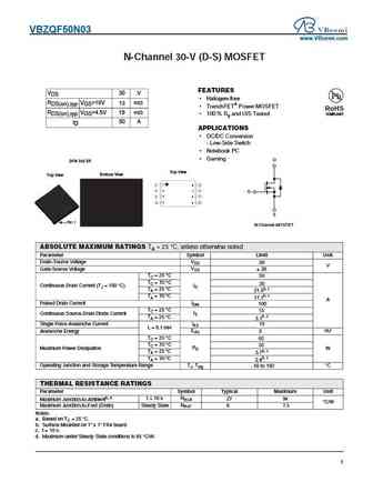
VBZQF50N03 www.VBsemi.com N-Channel 30-V (D-S) MOSFET FEATURES 30 V VDS Halogen-free RDS(on),typ VGS=10V 13 m TrenchFET Power MOSFET RoHS RDS(on),typ VGS=4.5V 19 m 100 % Rg and UIS Tested COMPLIANT ID 50 A APPLICATIONS DC/DC Conversion - Low-Side Switch Notebook PC Gaming D DFN 3x3 EP Top View Bottom View Top View 1 8 2 7 G 3 6
vbze50n03.pdf
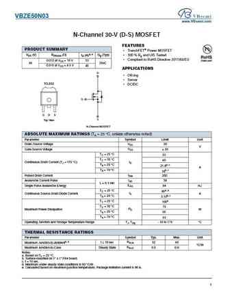
VBZE50N03 www.VBsemi.com N-Channel 30-V (D-S) MOSFET FEATURES PRODUCT SUMMARY TrenchFET Power MOSFET VDS (V) RDS(on) ( ) ID (A)a, e Qg (Typ) 100 % Rg and UIS Tested Compliant to RoHS Directive 2011/65/EU 0.010 at VGS = 10 V 53 30 28nC 0.016 at VGS = 4.5 V 40 APPLICATIONS D OR-ing Server TO-252 DC/DC G G D S S Top View N-Channel MOSFET ABSO
vbzl150n03.pdf
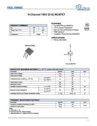
VBZL150N03 www.VBsemi.com N-Channel 150V (D-S) MOSFET FEATURES PRODUCT SUMMARY TrenchFET Power MOSFETs VDS 150 175 C Junction Temperature V New Low Thermal Resistance Package RDS(on) VGS = 10 V 35 m PWM Optimized ID 55 A Compliant to RoHS Directive 2002/95/EC Configuration Single APPLICATIONS Primary Side Switch D D2PAK (TO-263) G D G S S N-
vbzm150n03.pdf
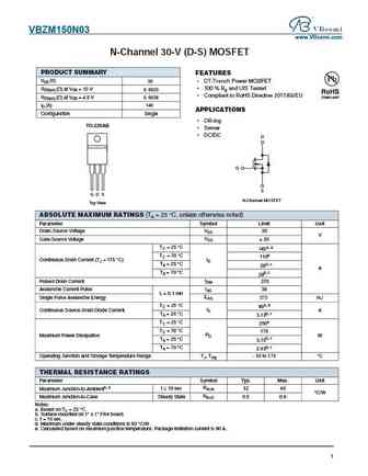
VBZM150N03 www.VBsemi.com N-Channel 30-V (D-S) MOSFET PRODUCT SUMMARY FEATURES VDS (V) 30 DT-Trench Power MOSFET 100 % Rg and UIS Tested RDS(on) ( ) at VGS = 10 V 0.0020 Compliant to RoHS Directive 2011/65/EU RDS(on) ( ) at VGS = 4.5 V 0.0028 ID (A) 140 APPLICATIONS Configuration Single OR-ing TO-220AB Server DC/DC D G S G D S N-Channel MOS
yjg50n03a.pdf
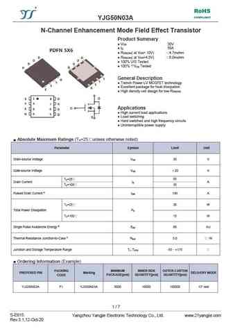
RoHS COMPLIANT YJG50N03A N-Channel Enhancement Mode Field Effect Transistor Product Summary V 30V DS I 50A D R ( at V = 10V) 4.7mohm DS(ON) GS R ( at V =4.5V) 6.0mohm DS(ON) GS 100% UIS Tested 100% V Tested DS General Description Trench Power LV MOSFET technology Excellent package for heat dissipation High density ce
yjd50n03a.pdf
RoHS COMPLIANT YJD50N03A N-Channel Enhancement Mode Field Effect Transistor Product Summary V 30V DS I 50A D R ( at V =10V) 9.0mohm DS(ON) GS R ( at V =4.5V) 11.0mohm DS(ON) GS 100% UIS Tested 100% VDS Tested General Description Trench Power LV MOSFET technology Excellent package for heat dissipation High density cell
hm150n03d.pdf
HM150N03 N-Channel Enhancement Mode Power MOSFET Description The 15 D uses advanced trench technology and design to provide excellent RDS(ON) with low gate charge. It can be used in a wide variety of applications. General Features VDS =30V,ID =150A RDS(ON)
hm150n03k.pdf
HM150N03K N-Channel Enhancement Mode Power MOSFET Description The 15 K uses advanced trench technology and design to provide excellent RDS(ON) with low gate charge. It can be used in a wide variety of applications. General Features VDS =30V,ID =150A RDS(ON)
hm50n03k.pdf
HM50N03K N-Channel Enhancement Mode Power MOSFET DESCRIPTION The HM50N03K uses advanced trench technology and design to provide excellent RDS(ON) with low gate charge. It can be used in a wide variety of applications. GENERAL FEATURES VDS =30V,ID =50A RDS(ON)
hm50n03i.pdf
N-Channel Enhancement Mode Power MOSFET Description The uses advanced trench technology and design to provide excellent RDS(ON) with low gate charge. It can be used in a wide variety of applications. General Features VDS =30V,ID =50A RDS(ON)
hm150n03.pdf
HM150N03 N-Channel Enhancement Mode Power MOSFET Description The HM150N03 uses advanced trench technology and design to provide excellent RDS(ON) with low gate charge. It can be used in a wide variety of applications. General Features VDS =30V,ID =150A RDS(ON)
ipd050n03l.pdf
isc N-Channel MOSFET Transistor IPD050N03L, IIPD050N03L FEATURES Static drain-source on-resistance RDS(on) 5m Enhancement mode 100% avalanche tested Minimum Lot-to-Lot variations for robust device performance and reliable operation DESCRITION Fast switching ABSOLUTE MAXIMUM RATINGS(T =25 ) a SYMBOL PARAMETER VALUE UNIT V Drain-Source Voltage 30 V DSS V Ga
ipu050n03l.pdf
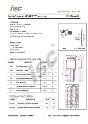
isc N-Channel MOSFET Transistor IPU050N03L FEATURES With TO-251(IPAK) packaging High speed switching Easy to use 100% avalanche tested Minimum Lot-to-Lot variations for robust device performance and reliable operation APPLICATIONS Power supply DC-DC converters Motor control Switching applications ABSOLUTE MAXIMUM RATINGS(T =25 ) a SYMBOL PARAMETER VALUE
spd50n03s2.pdf
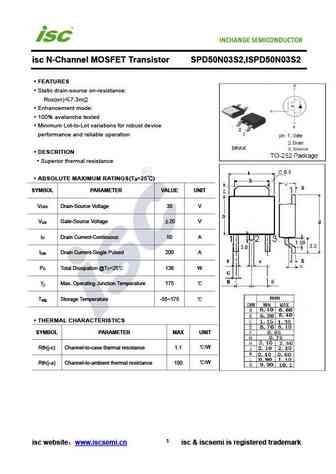
isc N-Channel MOSFET Transistor SPD50N03S2,ISPD50N03S2 FEATURES Static drain-source on-resistance RDS(on) 7.3m Enhancement mode 100% avalanche tested Minimum Lot-to-Lot variations for robust device performance and reliable operation DESCRITION Superior thermal resistance ABSOLUTE MAXIMUM RATINGS(T =25 ) a SYMBOL PARAMETER VALUE UNIT V Drain-Source Voltage 3
fdd050n03b.pdf
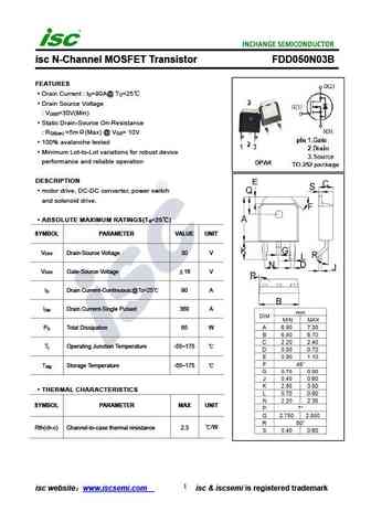
isc N-Channel MOSFET Transistor FDD050N03B FEATURES Drain Current I =90A@ T =25 D C Drain Source Voltage V =30V(Min) DSS Static Drain-Source On-Resistance R =5m (Max) @ V = 10V DS(on) GS 100% avalanche tested Minimum Lot-to-Lot variations for robust device performance and reliable operation DESCRIPTION motor drive, DC-DC converter, power switch and solenoid
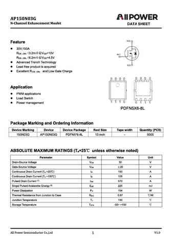
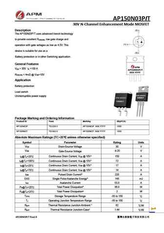
ap150n03d.pdf
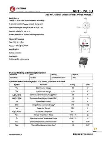
AP150N03D 30V N-Channel Enhancement Mode MOSFET Description The AP150N03D uses advanced trench technology to provide excellent R , low gate charge and DS(ON) operation with gate voltages as low as 4.5V. This device is suitable for use as a Battery protection or in other Switching application. General Features V = 30V I =150 A DS D R
ap150n03p ap150n03t.pdf
AP150N03PIT 30V N-Channel Enhancement Mode MOSFET Description The AP150N03P/T uses advanced trench technology to provide excellent R , low gate charge and DS(ON) operation with gate voltages as low as 4.5V. This device is suitable for use as a Battery protection or in other Switching application. General Features V = 30V I =150 A DS D R
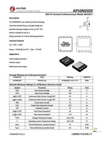
ap50n03df.pdf
AP50N03DF 30V N-Channel Enhancement Mode MOSFET Description The AP50N03DF uses advanced trench technology to provide excellent R , low gate charge and DS(ON) operation with gate voltages as low as 4.5V. This device is suitable for use as a Battery protection or in other Switching application. General Features V = 30V I =50A DS D R
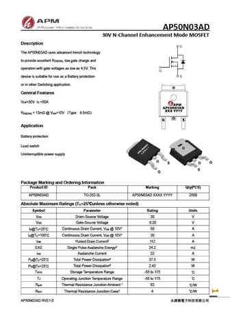
ap50n03ad.pdf
AP50N03AD 30V N-Channel Enhancement Mode MOSFET Description The AP50N03AD uses advanced trench technology to provide excellent R , low gate charge and DS(ON) operation with gate voltages as low as 4.5V. This device is suitable for use as a Battery protection or in other Switching application. General Features V =30V I =50A DS D R
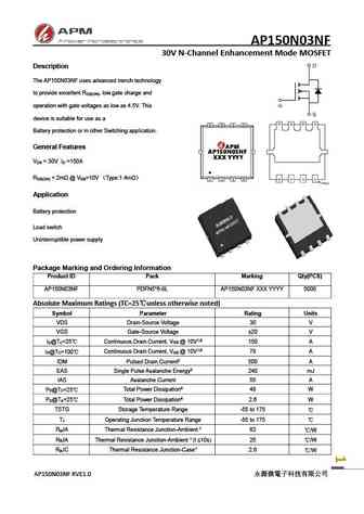
ap150n03nf.pdf
AP150N03NF 30V N-Channel Enhancement Mode MOSFET Description The AP150N03NF uses advanced trench technology to provide excellent R , low gate charge and DS(ON) operation with gate voltages as low as 4.5V. This device is suitable for use as a Battery protection or in other Switching application. General Features V = 30V I =150A DS D R
ap50n03s.pdf
AP50N03S 30V N-Channel Enhancement Mode MOSFET Description The AP50N03S uses advanced trench technology to provide excellent R , low gate charge and DS(ON) operation with gate voltages as low as 4.5V. This device is suitable for use as a Battery protection or in other Switching application. General Features V = 30V I =50 A DS D R
ap50n03d.pdf
AP50N03D 30V N-Channel Enhancement Mode MOSFET Description The AP50N03D uses advanced trench technology to provide excellent R , low gate charge and DS(ON) operation with gate voltages as low as 4.5V. This device is suitable for use as a Battery protection or in other Switching application. General Features V = 30V I =50 A DS D R
Otros transistores... 3205PL , 3205TR , 3400L , 3401A , 3401L , 40N10K , 40P04 , 45P40 , IRLB3034 , 5P40 , 60N04 , 6706A , 68P40 , 80N03 , 80N04 , 80N08TR , 8205A .
🌐 : EN ES РУ

Liste
Recientemente añadidas las descripciónes de los transistores:
MOSFET: ASU70R600E | ASU65R850E | ASU65R550E | ASU65R350E | ASR65R120EFD | ASR65R046EFD | ASQ65R046EFD | ASM65R280E | ASM60R330E | ASE70R950E | ASD80R750E | ASD70R950E | ASD70R600E | ASD70R380E | ASD65R850E | ASD65R550E
Popular searches
irfp460 характеристики | k2837 datasheet | k389 transistor | mje15032g equivalent | nsd134 | 60r190p datasheet | cs30n20 datasheet | go42n10