FTK2341E MOSFET Equivalente. Reemplazo. Hoja de especificaciones. Principales características
Número de Parte: FTK2341E
Tipo de FET: MOSFET
Polaridad de transistor: P
ESPECIFICACIONES MÁXIMAS
Pdⓘ - Máxima disipación de potencia: 1.4 W
|Vds|ⓘ - Voltaje máximo drenador-fuente: 20 V
|Vgs|ⓘ - Voltaje máximo fuente-puerta: 8 V
|Id|ⓘ - Corriente continua de drenaje: 4 A
Tjⓘ - Temperatura máxima de unión: 150 °C
CARACTERÍSTICAS ELÉCTRICAS
trⓘ - Tiempo de subida: 17 nS
Cossⓘ - Capacitancia de salida: 200 pF
RDSonⓘ - Resistencia estado encendido drenaje a fuente: 0.043 Ohm
Encapsulados: SOT23
Búsqueda de reemplazo de FTK2341E MOSFET
- Selecciónⓘ de transistores por parámetros
FTK2341E datasheet
ftk2341e.pdf
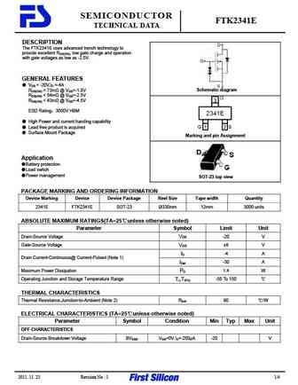
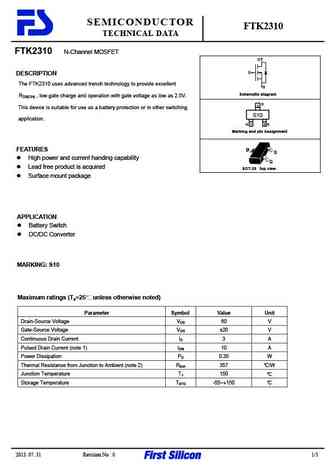
SEMICONDUCTOR FTK2341E TECHNICAL DATA DESCRIPTION The FTK2341E uses advanced trench technology to provide excellent RDS(ON), low gate charge and operation with gate voltages as low as -2.5V. GENERAL FEATURES VDS = -20V,ID =-4A Schematic diagram RDS(ON)
ftk2306a.pdf
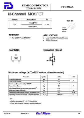
SEMICONDUCTOR FTK2306A TECHNICAL DATA N-Channel MOSFET ID V(BR)DSS RDS(on)MAX SOT-23 47m @10V 30V 3.16A 65m @4.5V 1. GATE 2. SOURCE 3. DRAIN FEATURE APPLICATION TrenchFET Power MOSFET Load Switch for Portable Devices DC/DC Converter MARKING Equivalent Circuit Maximum ratings (at TA=25 unless otherwise noted) Parameter Symbol Value Unit Drain-Source
ftk2304.pdf
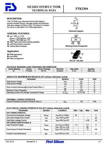
SEMICONDUCTOR FTK2304 TECHNICAL DATA D DESCRIPTION The FTK2304 uses advanced trench technology to G provide excellent RDS(ON), low gate charge and operation with gate voltages as low as 4.5V. This device is suitable for use as a load switch or in PWM applications. S Schematic diagram GENERAL FEATURES D VDS = 30V ,ID = 3.3A 3 RDS(ON)
ftk2302.pdf
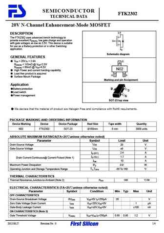
SEMICONDUCTOR FTK2302 TECHNICAL DATA 20V N-Channel Enhancement-Mode MOSFET D DESCRIPTION The FTK2302 uses advanced trench technology to provide excellent RDS(ON), low gate charge and operation G with gate voltages as low as 2.5V. This device is suitable for use as a Battery protection or in other Switching application. S Schematic diagram GENERAL FEATURES VDS = 20V,I
Otros transistores... FTK2302, FTK2304, FTK2306, FTK2306A, FTK2310, FTK2312, FTK2324, FTK2333, EMB04N03H, FTK25N03PDFN33, FTK2627, FTK2816E, FTK3004D, FTK3018, FTK3022, FTK3051, FTK3134K
History: TSG120N10AT | TPCC8A01-H
🌐 : EN ES РУ

Liste
Recientemente añadidas las descripciónes de los transistores:
MOSFET: SVF11N65F | SVF11N65T | FKBB3105 | EHBA036R1 | CRTT067N10N | AP6NA3R2MT | AP65SA145DDT8 | AP4NAR95CMT-A | AP4024GEMT-HF | AP3P050AH | AP3P020H | AP3N9R5YT | AP3N9R5MT | AP3N5R0MT | AP2P053Y | AP12A390YT
Popular searches
2sc536 | d718 transistor | irfp250n datasheet | 2n5550 | 2sd1047 | 2n3035 | ksc1815 | bu406