FTK3415 MOSFET Equivalente. Reemplazo. Hoja de especificaciones. Principales características
Número de Parte: FTK3415
Tipo de FET: MOSFET
Polaridad de transistor: P
ESPECIFICACIONES MÁXIMAS
Pdⓘ - Máxima disipación de potencia: 1.5 W
|Vds|ⓘ - Voltaje máximo drenador-fuente: 20 V
|Vgs|ⓘ - Voltaje máximo fuente-puerta: 8 V
|Id|ⓘ - Corriente continua de drenaje: 4 A
Tjⓘ - Temperatura máxima de unión: 150 °C
CARACTERÍSTICAS ELÉCTRICAS
trⓘ - Tiempo de subida: 17 nS
Cossⓘ - Capacitancia de salida: 205 pF
RDSonⓘ - Resistencia estado encendido drenaje a fuente: 0.06 Ohm
Encapsulados: SOT23
Búsqueda de reemplazo de FTK3415 MOSFET
- Selecciónⓘ de transistores por parámetros
FTK3415 datasheet
ftk3415.pdf
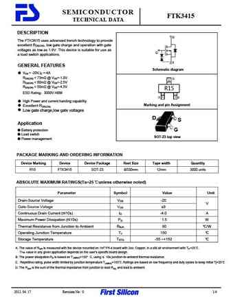
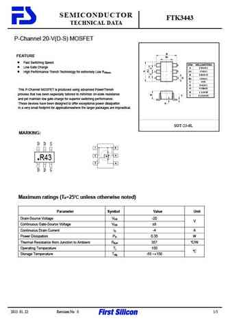
SEMICONDUCTOR FTK3415 TECHNICAL DATA DESCRIPTION D The FTK3415 uses advanced trench technology to provide excellent RDS(ON), low gate charge and operation with gate voltages as low as 1.8V. This device is suitable for use as G a load switch applications. S GENERAL FEATURES Schematic diagram VDS = -20V,ID =-4A RDS(ON)
ftk3415l.pdf
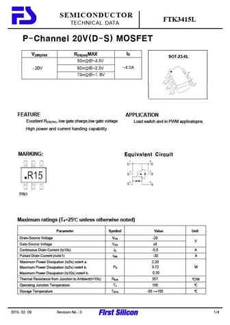
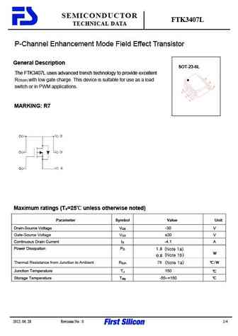
SEMICONDUCTOR FTK3415L TECHNICAL DATA P-Channel 20V(D-S) MOSFET ID V(BR)DSS RDS(on)MAX SOT-23-6L 50m @-4.5V -4.0A -20V 60m @-2.5V 73m @-1. 8V FEATURE APPLICATION Excellent RDS(ON), low gate charge,low gate voltage Load switch and in PWM applicatopns High power and current handing capability MARKING Equivalent Circuit PIN1 Maximum ratings (Ta=25 unless otherwise
ftk3400.pdf
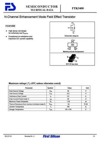
SEMICONDUCTOR FTK3400 TECHNICAL DATA N-Channel Enhancement Mode Field Effect Transistor D FEATURE G High dense cell design for extremely low R S DS(ON) Schematic diagram Exceptional on-resistance and maximum DC current capability D 3 R0 G 1 2 S Marking and pin Assignment SOT-23 top view Maximum ratings ( Ta=25 unless otherwise noted) Parameter Symbol Value Unit
ftk3404.pdf
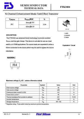
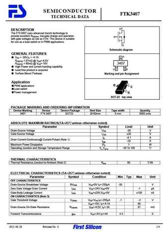
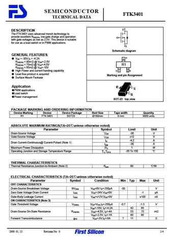
SEMICONDUCTOR FTK3404 TECHNICAL DATA N-Channel Enhancement Mode Field Effect Transistor ID V(BR)DSS RDS(on)MAX 3 30m @ 10V 30V 5.8A 2 1 42m @4.5V SOT 23 1. GATE DESCRIPTION 2. SOURCE 3. DRAIN The FTK3404 use advanced trench technology to provide excellent RDS(ON) and low gate charge. This device is suit able for use as a load switch or in PWM applications.The s
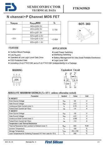
Otros transistores... FTK3134KD, FTK3139K, FTK3341, FTK3400, FTK3401, FTK3404, FTK3407, FTK3407L, IRFP460, FTK3415L, FTK3439KD, FTK3443, FTK35N03PDFN33, FTK35N03PDFN56, FTK3610, FTK3615, FTK3620
History: TPV65R080C
🌐 : EN ES РУ

Liste
Recientemente añadidas las descripciónes de los transistores:
MOSFET: AUW033N08BG | AUW025N10 | AUR030N10 | AUR020N10 | AUR020N085 | AUR014N10 | AUP074N10 | AUP065N10 | AUP062N08BG | AUP060N08AG | HYG053N10NS1B | HYG053N10NS1P | AP220N04T | AP220N04P | QM3126M3 | AUP060N055
Popular searches
irf640 datasheet | c945 transistor equivalent | irfz44 datasheet | tip3055 transistor | irf530 datasheet | 2sc2625 | 2sc1815 transistor | 2sd718