IRF630S Datasheet. Equivalente. Reemplazo. Hoja de especificaciones. Principales características
Número de Parte: IRF630S 📄📄
Tipo de FET: MOSFET
Polaridad de transistor: N
ESPECIFICACIONES MÁXIMAS
Pdⓘ - Máxima disipación de potencia: 70 W
|Vds|ⓘ - Voltaje máximo drenador-fuente: 200 V
|Vgs|ⓘ - Voltaje máximo fuente-puerta: 20 V
|Id|ⓘ - Corriente continua de drenaje: 9 A
Tjⓘ - Temperatura máxima de unión: 150 °C
CARACTERÍSTICAS ELÉCTRICAS
trⓘ - Tiempo de subida: 15 nS
Cossⓘ - Capacitancia de salida: 90 pF
RDSonⓘ - Resistencia estado encendido drenaje a fuente: 0.4 Ohm
Encapsulados: TO263
📄📄 Copiar
Búsqueda de reemplazo de IRF630S MOSFET
- Selecciónⓘ de transistores por parámetros
IRF630S datasheet
..1. Size:981K international rectifier
irf630spbf.pdf 
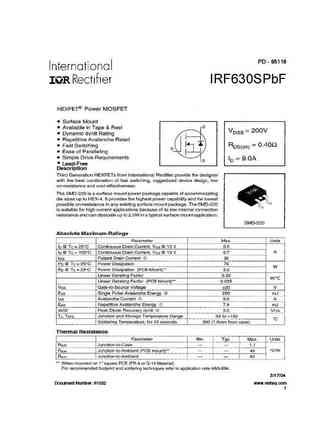
PD - 95118 IRF630SPbF Lead-Free 3/17/04 Document Number 91032 www.vishay.com 1 IRF630SPbF Document Number 91032 www.vishay.com 2 IRF630SPbF Document Number 91032 www.vishay.com 3 IRF630SPbF Document Number 91032 www.vishay.com 4 IRF630SPbF Document Number 91032 www.vishay.com 5 IRF630SPbF Document Number 91032 www.vishay.com 6 IRF630SPbF D2Pak Package Outli
..2. Size:85K st
irf630s.pdf
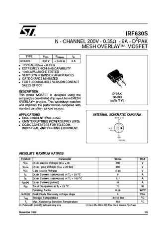
IRF630S N - CHANNEL 200V - 0.35 - 9A- D2PAK MESH OVERLAY MOSFET TYPE VDSS RDS(on) ID IRF630S 200 V
..3. Size:196K vishay
irf630spbf sihf630s.pdf
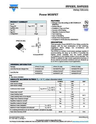
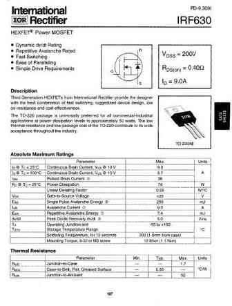
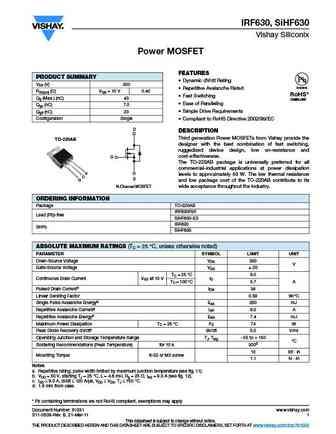
IRF630S, SiHF630S Vishay Siliconix Power MOSFET FEATURES PRODUCT SUMMARY Halogen-free According to IEC 61249-2-21 VDS (V) 200 Definition RDS(on) ( )VGS = 10 V 0.40 Surface Mount Qg (Max.) (nC) 43 Available in Tape and Reel Qgs (nC) 7.0 Dynamic dV/dt Rating Qgd (nC) 23 Repetitive Avalanche Rated Configuration Single Fast Switching Ease of Paralleli
..4. Size:170K vishay
irf630s sihf630s.pdf

IRF630S, SiHF630S Vishay Siliconix Power MOSFET FEATURES PRODUCT SUMMARY Halogen-free According to IEC 61249-2-21 VDS (V) 200 Definition RDS(on) ( )VGS = 10 V 0.40 Surface Mount Qg (Max.) (nC) 43 Available in Tape and Reel Qgs (nC) 7.0 Dynamic dV/dt Rating Qgd (nC) 23 Repetitive Avalanche Rated Configuration Single Fast Switching Ease of Paralleli
..5. Size:1779K kexin
irf630s.pdf
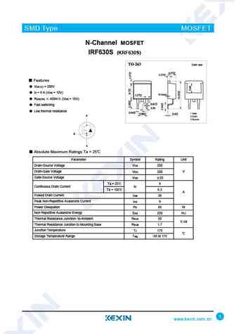
SMD Type MOSFET N-Channel MOSFET IRF630S (KRF630S) Features VDS (V) = 200V ID = 9 A (VGS = 10V) RDS(ON) 400m (VGS = 10V) Fast switching Low thermal resistance d g s Absolute Maximum Ratings Ta = 25 Parameter Symbol Rating Unit Drain-Source Voltage VDS 200 V Drain-Gate Voltage VDG 200 Gate-Source Voltage VGS 20 Ta = 25 9 Cont
..6. Size:1808K cn vbsemi
irf630s.pdf
IRF630S www.VBsemi.tw Power MOSFET FEATURES PRODUCT SUMMARY Halogen-free According to IEC 61249-2-21 VDS (V) 200 Definition RDS(on) ( )VGS = 10 V 0.30 Surface Mount Qg (Max.) (nC) 43 Available in Tape and Reel Qgs (nC) 7.0 Dynamic dV/dt Rating Qgd (nC) 23 Repetitive Avalanche Rated Configuration Single Fast Switching Ease of Paralleling Simpl
8.2. Size:859K 1
irf630b irfs630b.pdf

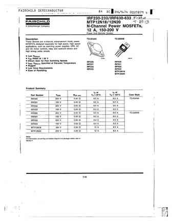
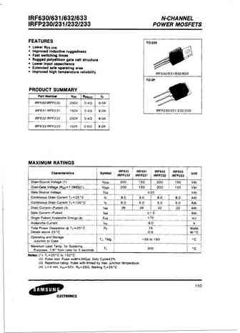
IRF630B/IRFS630B 200V N-Channel MOSFET General Description Features These N-Channel enhancement mode power field effect 9.0A, 200V, RDS(on) = 0.4 @VGS = 10 V transistors are produced using Fairchild s proprietary, Low gate charge ( typical 22 nC) planar, DMOS technology. Low Crss ( typical 22 pF) This advanced technology has been especially tailored to Fast switchin
8.4. Size:335K international rectifier
irf630npbf irf630nspbf irf630nlpbf.pdf

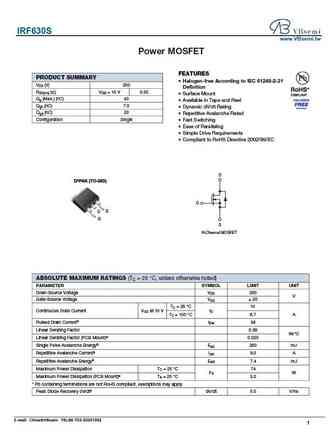
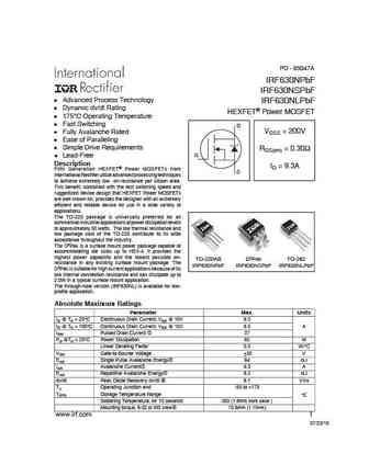
PD - 95047A IRF630NPbF IRF630NSPbF l Advanced Process Technology IRF630NLPbF l Dynamic dv/dt Rating HEXFET Power MOSFET l 175 C Operating Temperature l Fast Switching D VDSS = 200V l Fully Avalanche Rated l Ease of Paralleling l Simple Drive Requirements RDS(on) = 0.30 G l Lead-Free Description ID = 9.3A Fifth Generation HEXFET Power MOSFETs from S International Rec
8.5. Size:335K international rectifier
irf630nlpbf irf630npbf irf630nspbf irf630nstrrpbf.pdf
PD - 95047A IRF630NPbF IRF630NSPbF l Advanced Process Technology IRF630NLPbF l Dynamic dv/dt Rating HEXFET Power MOSFET l 175 C Operating Temperature l Fast Switching D VDSS = 200V l Fully Avalanche Rated l Ease of Paralleling l Simple Drive Requirements RDS(on) = 0.30 G l Lead-Free Description ID = 9.3A Fifth Generation HEXFET Power MOSFETs from S International Rec
8.6. Size:155K international rectifier
irf630n.pdf
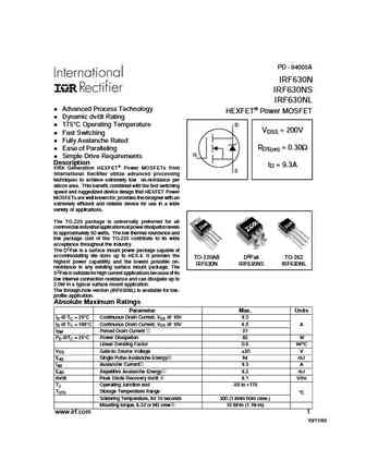
PD - 94005A IRF630N IRF630NS IRF630NL Advanced Process Technology HEXFET Power MOSFET Dynamic dv/dt Rating 175 C Operating Temperature D VDSS = 200V Fast Switching Fully Avalanche Rated RDS(on) = 0.30 Ease of Paralleling G Simple Drive Requirements Description ID = 9.3A Fifth Generation HEXFET Power MOSFETs from S International Rectifier utilize advanced proces
8.7. Size:1372K international rectifier
irf630pbf.pdf
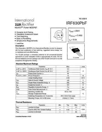
PD- 95916 IRF630PbF Lead-Free 9/27/04 Document Number 91031 www.vishay.com 1 IRF630PbF Document Number 91031 www.vishay.com 2 IRF630PbF Document Number 91031 www.vishay.com 3 IRF630PbF Document Number 91031 www.vishay.com 4 IRF630PbF Document Number 91031 www.vishay.com 5 IRF630PbF Document Number 91031 www.vishay.com 6 IRF630PbF Peak Diode Recovery dv/dt T
8.8. Size:99K philips
irf630 s 1.pdf
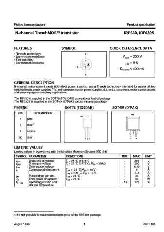
Philips Semiconductors Product specification N-channel TrenchMOS transistor IRF630, IRF630S FEATURES SYMBOL QUICK REFERENCE DATA Trench technology d Low on-state resistance VDSS = 200 V Fast switching Low thermal resistance ID = 9 A g RDS(ON) 400 m s GENERAL DESCRIPTION N-channel, enhancement mode field-effect power transistor using Trench technology
8.9. Size:104K st
irf630.pdf
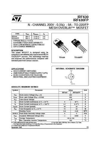
IRF630 IRF630FP N - CHANNEL 200V - 0.35 - 9A - TO-220/FP MESH OVERLAY MOSFET TYPE VDSS RDS(on) ID IRF630 200 V
8.10. Size:434K st
irf630mfp.pdf
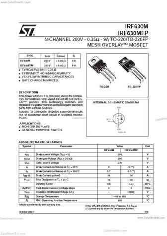
www.DataSheet4U.com IRF630M IRF630MFP N-CHANNEL 200V - 0.35 - 9A TO-220/TO-220FP MESH OVERLAY MOSFET TYPE VDSS RDS(on) ID IRF630M 200 V
8.11. Size:343K st
irf630m.pdf
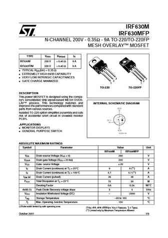
IRF630M IRF630MFP N-CHANNEL 200V - 0.35 - 9A TO-220/TO-220FP MESH OVERLAY MOSFET TYPE VDSS RDS(on) ID IRF630M 200 V
8.12. Size:339K st
irf630 irf630fp.pdf
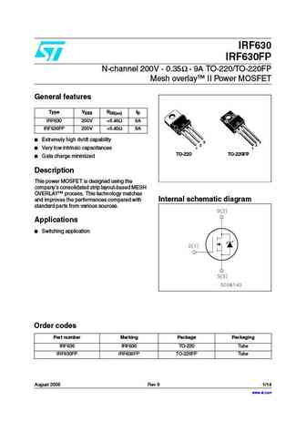
IRF630 IRF630FP N-channel 200V - 0.35 - 9A TO-220/TO-220FP Mesh overlay II Power MOSFET General features Type VDSS RDS(on) ID IRF630 200V
8.15. Size:129K fairchild semi
irf630 rf1s630sm.pdf
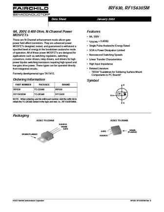
IRF630, RF1S630SM Data Sheet January 2002 9A, 200V, 0.400 Ohm, N-Channel Power Features MOSFETs 9A, 200V These are N-Channel enhancement mode silicon gate rDS(ON) = 0.400 power field effect transistors. They are advanced power Single Pulse Avalanche Energy Rated MOSFETs designed, tested, and guaranteed to withstand a specified level of energy in the breakdown avalanc
8.16. Size:859K fairchild semi
irf630b.pdf
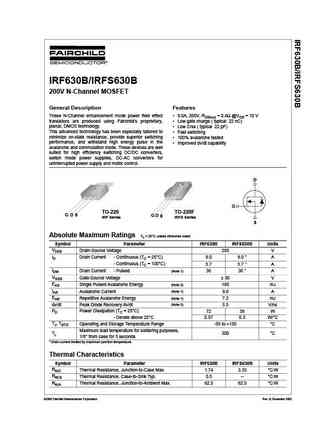
IRF630B/IRFS630B 200V N-Channel MOSFET General Description Features These N-Channel enhancement mode power field effect 9.0A, 200V, RDS(on) = 0.4 @VGS = 10 V transistors are produced using Fairchild s proprietary, Low gate charge ( typical 22 nC) planar, DMOS technology. Low Crss ( typical 22 pF) This advanced technology has been especially tailored to Fast switchin
8.18. Size:945K samsung
irf630a.pdf
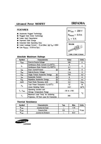
Advanced Power MOSFET FEATURES BVDSS = 200 V Avalanche Rugged Technology RDS(on) = 0.4 Rugged Gate Oxide Technology Lower Input Capacitance ID = 9 A Improved Gate Charge Extended Safe Operating Area Lower Leakage Current 10 A (Max.) @ VDS = 200V Low RDS(ON) 0.333 (Typ.) 1 2 3 1.Gate 2. Drain 3. Source Absolute Maximum Ratings Symbol Characteristic Value
8.19. Size:203K vishay
irf630pbf sihf630.pdf
IRF630, SiHF630 Vishay Siliconix Power MOSFET FEATURES PRODUCT SUMMARY Dynamic dV/dt Rating VDS (V) 200 Available Repetitive Avalanche Rated RDS(on) ( )VGS = 10 V 0.40 RoHS* Fast Switching Qg (Max.) (nC) 43 COMPLIANT Ease of Paralleling Qgs (nC) 7.0 Qgd (nC) 23 Simple Drive Requirements Configuration Single Compliant to RoHS Directive 2002/95/EC D D
8.20. Size:575K vishay
irf630 sihf630.pdf
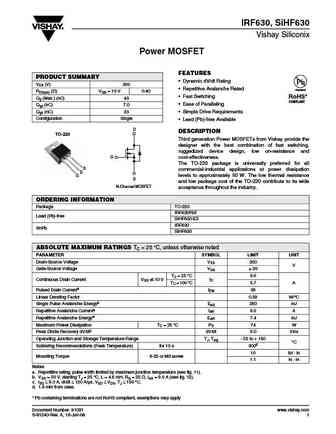
IRF630, SiHF630 Vishay Siliconix Power MOSFET FEATURES PRODUCT SUMMARY Dynamic dV/dt Rating VDS (V) 200 Repetitive Avalanche Rated Available RDS(on) ( )VGS = 10 V 0.40 Fast Switching RoHS* Qg (Max.) (nC) 43 COMPLIANT Ease of Paralleling Qgs (nC) 7.0 Qgd (nC) 23 Simple Drive Requirements Configuration Single Lead (Pb)-free Available D DESCRIPTION TO-
8.22. Size:75K hsmc
hirf630.pdf
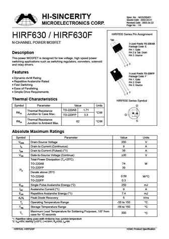
Spec. No. MOS200401 HI-SINCERITY Issued Date 2004.04.01 Revised Date 2005.04.22 MICROELECTRONICS CORP. Page No. 1/6 HIRF630 Series Pin Assignment HIRF630 / HIRF630F Tab N-CHANNEL POWER MOSFET 3-Lead Plastic TO-220AB Package Code E Pin 1 Gate Pin 2 & Tab Drain Description Pin 3 Source This power MOSFET is designed for low voltage, high speed power switching applicati
8.23. Size:94K ape
irf630.pdf
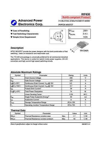
IRF630 RoHS-compliant Product Advanced Power N-CHANNEL ENHANCEMENT MODE Electronics Corp. POWER MOSFET Ease of Paralleling D BVDSS 200V Fast Switching Characteristic RDS(ON) 0.4 Simple Drive Requirement ID 9.0A G S Description G TO-220(P) D APEC MOSFET provide the power designer with the best combination of fast S switching , lower on-resistance and reasonable cost.
8.24. Size:594K nell
irf630h.pdf
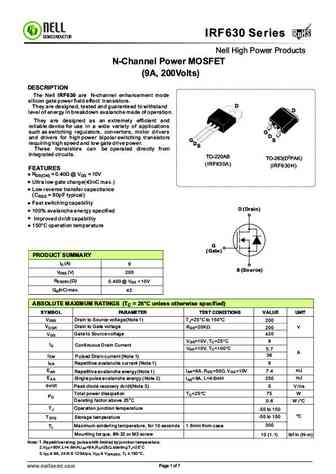
RoHS IRF630 Series RoHS SEMICONDUCTOR Nell High Power Products N-Channel Power MOSFET (9A, 200Volts) DESCRIPTION The Nell IRF630 are N-channel enhancement mode silicon gate power field effect transistors. D They are designed, tested and guaranteed to withstand D level of energy in breakdown avalanche made of operation. They are designed as an extremely efficient and reliab
8.25. Size:2999K cn vbsemi
irf630mfp.pdf
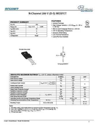
IRF630MFP www.VBsemi.tw N-Channel 200 V (D-S) MOSFET FEATURES PRODUCT SUMMARY Isolated Package VDS (V) 200 Available High Voltage Isolation = 2.5 kVRMS (t = 60 s; RDS(on) ( )VGS = 10 V 0.265 f = 60 Hz) RoHS Qg (Max.) (nC) 16 Sink to Lead Creepage Distance = 4.8 mm 175 C Operating Temperature Qgs (nC) 5 Dynamic dV/dt Rating Qgd (nC) 8 Low Thermal Resist
8.26. Size:2683K cn vbsemi
irf630p.pdf
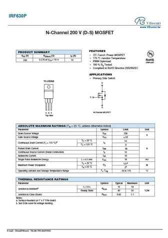
IRF630P www.VBsemi.tw N-Channel 200 V (D-S) MOSFET FEATURES PRODUCT SUMMARY DT-Trench Power MOSFET VDS (V) RDS(on) ( )ID (A) 175 C Junction Temperature 0.270 at VGS =10V 10 200 PWM Optimized 100 % Rg Tested Compliant to RoHS Directive 2002/95/EC APPLICATIONS Primary Side Switch TO-220AB D G S N-Channel MOSFET G D S Top View ABSOLUTE MAXIMUM RATI
8.27. Size:114K inchange semiconductor
irf630.pdf
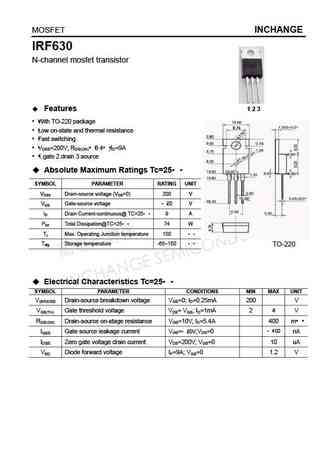
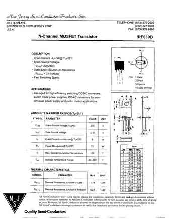
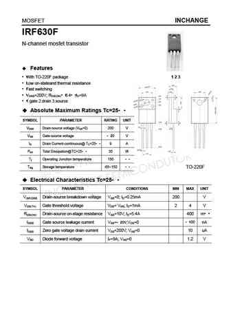
MOSFET INCHANGE IRF630 N-channel mosfet transistor Features 1 2 3 With TO-220 package Low on-state and thermal resistance Fast switching VDSS=200V; RDS(ON) 0.4 ;ID=9A 1.gate 2.drain 3.source Absolute Maximum Ratings Tc=25 SYMBOL PARAMETER RATING UNIT VDSS Drain-source voltage (VGS=0) 200 V VGS Gate-source voltage 20 V ID Drain Current-continuous@ TC
8.28. Size:142K inchange semiconductor
irf630b.pdf
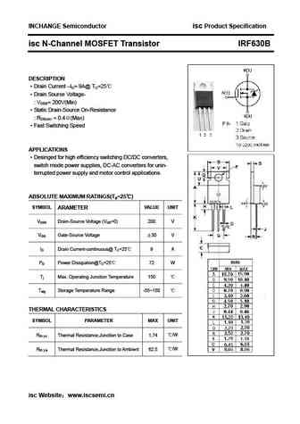
INCHANGE Semiconductor isc Product Specification isc N-Channel MOSFET Transistor IRF630B DESCRIPTION Drain Current ID= 9A@ TC=25 Drain Source Voltage- VDSS= 200V(Min) Static Drain-Source On-Resistance RDS(on) = 0.4 (Max) Fast Switching Speed APPLICATIONS Desinged for high efficiency switching DC/DC converters, switch mode power supplies, DC-AC conve
8.29. Size:245K inchange semiconductor
irf630a.pdf
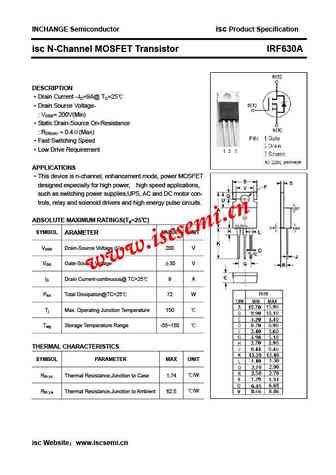
INCHANGE Semiconductor isc Product Specification isc N-Channel MOSFET Transistor IRF630A DESCRIPTION Drain Current ID=9A@ TC=25 Drain Source Voltage- VDSS= 200V(Min) Static Drain-Source On-Resistance RDS(on) = 0.4 (Max) Fast Switching Speed Low Drive Requirement APPLICATIONS This device is n-channel, enhancement mode, power MOSFET designed espec
8.30. Size:244K inchange semiconductor
irf630nl.pdf
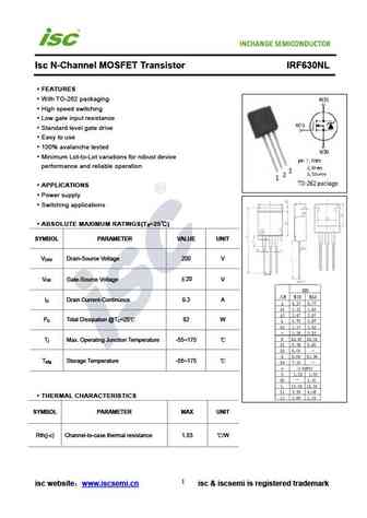
Isc N-Channel MOSFET Transistor IRF630NL FEATURES With TO-262 packaging High speed switching Low gate input resistance Standard level gate drive Easy to use 100% avalanche tested Minimum Lot-to-Lot variations for robust device performance and reliable operation APPLICATIONS Power supply Switching applications ABSOLUTE MAXIMUM RATINGS(T =25 ) a SYMBOL PAR
8.31. Size:232K inchange semiconductor
irf630nstrrpbf.pdf
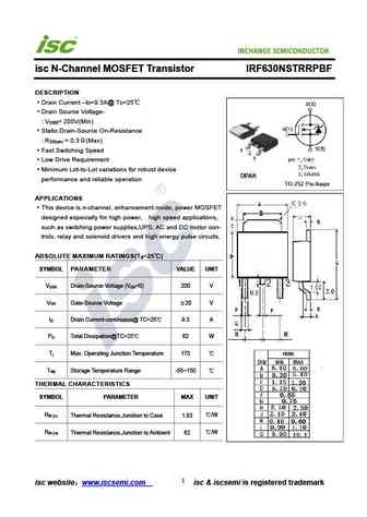
INCHANGE Semiconductor isc N-Channel MOSFET Transistor IRF630NSTRRPBF DESCRIPTION Drain Current I =9.3A@ T =25 D C Drain Source Voltage- V = 200V(Min) DSS Static Drain-Source On-Resistance R = 0.3 (Max) DS(on) Fast Switching Speed Low Drive Requirement Minimum Lot-to-Lot variations for robust device performance and reliable operation APPLICATIONS This de
8.32. Size:229K inchange semiconductor
irf630ns.pdf
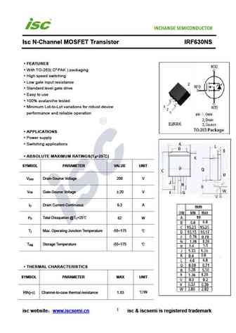
Isc N-Channel MOSFET Transistor IRF630NS FEATURES With TO-263( D PAK ) packaging High speed switching Low gate input resistance Standard level gate drive Easy to use 100% avalanche tested Minimum Lot-to-Lot variations for robust device performance and reliable operation APPLICATIONS Power supply Switching applications ABSOLUTE MAXIMUM RATINGS(T =25 ) a
8.33. Size:245K inchange semiconductor
irf630n.pdf
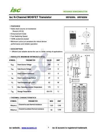
isc N-Channel MOSFET Transistor IRF630N IIRF630N FEATURES Static drain-source on-resistance RDS(on) 0.3 Enhancement mode Fast Switching Speed 100% avalanche tested Minimum Lot-to-Lot variations for robust device performance and reliable operation DESCRIPTION Efficient and reliable device for use in a wide variety of applications ABSOLUTE MAXIMUM RATINGS(T
8.34. Size:108K inchange semiconductor
irf630f.pdf
MOSFET INCHANGE IRF630F N-channel mosfet transistor Features With TO-220F package 1 2 3 Low on-stateand thermal resistance Fast switching VDSS=200V; RDS(ON) 0.4 ;ID=9A 1.gate 2.drain 3.source Absolute Maximum Ratings Tc=25 SYMBOL PARAMETER RATING UNIT VDSS Drain-source voltage (VGS=0) 200 V VGS Gate-source voltage 20 V ID Drain Current-continuous@ TC
Otros transistores... IRF623, IRF624, IRF624A, IRF624S, IRF625, IRF630, IRF630A, IRF630FI, TK10A60D, IRF631, IRF632, IRF633, IRF634, IRF634A, IRF634S, IRF635, IRF636A