SM3405NSQG MOSFET Equivalente. Reemplazo. Hoja de especificaciones. Principales características
Número de Parte: SM3405NSQG
Tipo de FET: MOSFET
Polaridad de transistor: N
ESPECIFICACIONES MÁXIMAS
Pdⓘ - Máxima disipación de potencia: 62.5
W
|Vds|ⓘ - Voltaje máximo drenador - fuente: 30
V
|Vgs|ⓘ - Voltaje máximo fuente - puerta: 12
V
|Id|ⓘ - Corriente continua de drenaje: 50
A
Tjⓘ - Temperatura máxima de unión: 150
°C
CARACTERÍSTICAS ELÉCTRICAS
trⓘ - Tiempo de subida: 12.2
nS
Cossⓘ - Capacitancia
de salida: 510
pF
Rds(on)ⓘ - Resistencia estado encendido drenaje a fuente: 0.0032
Ohm
Paquete / Cubierta: DFN3.3X3.3B-8
Búsqueda de reemplazo de SM3405NSQG MOSFET
-
Selección ⓘ de transistores por parámetros
SM3405NSQG datasheet
..1. Size:165K sino
sm3405nsqg.pdf 

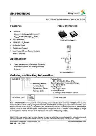
SM3405NSQG N-Channel Enhancement Mode MOSFET Features Pin Description D D D 30V/50A, D RDS(ON) = 3.2m (max.) @ VGS =4.5V RDS(ON) = 4m (max.) @ VGS =2.5V G S S S ESD protection DFN3.3x3.3-8(Saw-EP) 100% UIS + Rg Tested Avalanche Rated (5,6,7,8) DDDD Reliable and Rugged Lead Free and Green Devices Available (RoHS Compliant) (4) G Applications Power Managemen
8.1. Size:851K globaltech semi
gsm3405.pdf 

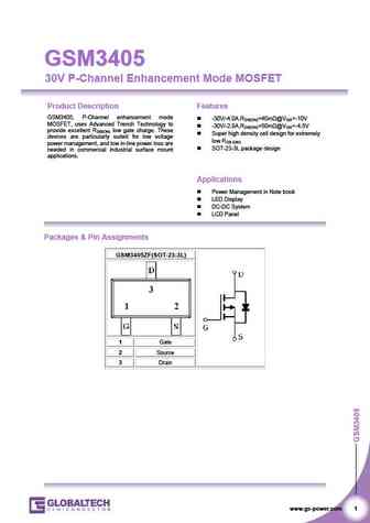
GSM3405 GSM3405 30V P-Channel Enhancement Mode MOSFET Product Description Features GSM3405, P-Channel enhancement mode -30V/-4.0A,RDS(ON)=40m @VGS=-10V MOSFET, uses Advanced Trench Technology to -30V/-2.8A,RDS(ON)=50m @VGS=-4.5V provide excellent RDS(ON) low gate charge. These Super high density cell design for extremely devices are particularly suited for low
9.1. Size:242K taiwansemi
tsm3400cx.pdf 

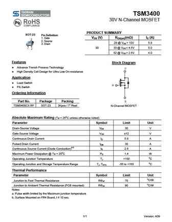
TSM3400 30V N-Channel MOSFET PRODUCT SUMMARY SOT-23 Pin Definition VDS (V) RDS(on)(m ) ID (A) 1. Gate 2. Source 28 @ VGS = 10V 5.8 3. Drain 30 33 @ VGS = 4.5V 5.0 52 @ VGS = 2.5V 4.0 Features Block Diagram Advance Trench Process Technology High Density Cell Design for Ultra Low On-resistance Application Load Switch PA Switch Ordering Infor
9.2. Size:235K taiwansemi
tsm3401cx.pdf 

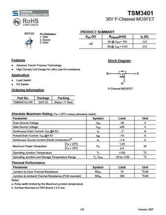
TSM3401 30V P-Channel MOSFET PRODUCT SUMMARY SOT-23 Pin Definition 1. Gate VDS (V) RDS(on)(m ) ID (A) 2. Source 60 @ VGS = 10V -3.0 3. Drain -30 90 @ VGS = 4.5V -2.0 Features Block Diagram Advance Trench Process Technology High Density Cell Design for Ultra Low On-resistance Application Load Switch PA Switch P-Channel MOSFET Ordering Info
9.3. Size:338K taiwansemi
tsm3404cx.pdf 

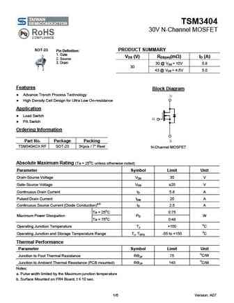
TSM3404 30V N-Channel MOSFET SOT-23 PRODUCT SUMMARY Pin Definition 1. Gate VDS (V) RDS(on)(m ) ID (A) 2. Source 3. Drain 30 @ VGS = 10V 5.8 30 43 @ VGS = 4.5V 5.0 Features Block Diagram Advance Trench Process Technology High Density Cell Design for Ultra Low On-resistance Application Load Switch PA Switch Ordering Information Part No. Pac
9.4. Size:165K sino
sm3403psqg.pdf 

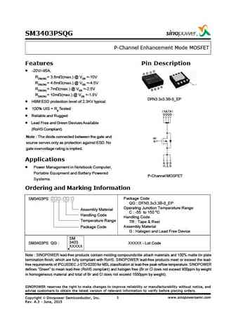
SM3403PSQG P-Channel Enhancement Mode MOSFET Features Pin Description -20V/-95A, D D D D RDS(ON) = 3.6m (max.) @ VGS =-10V RDS(ON) = 4.6m (max.) @ VGS =-4.5V G S RDS(ON) = 7m (max.) @ VGS =-2.5V S S RDS(ON) = 10m (max.) @ VGS =-1.8V DFN3.3x3.3B-8_EP HBM ESD protection level of 2.3KV typical 100% UIS + Rg Tested ( 5,6,7,8 ) DDDD Reliable and Rugged Lead Free
9.5. Size:154K sino
sm3406nsqg.pdf 

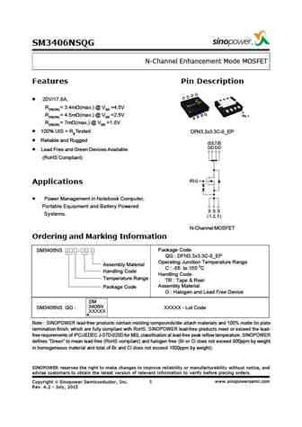
SM3406NSQG N-Channel Enhancement Mode MOSFET Features Pin Description D D D D 20V/17.8A, RDS(ON) = 3.4m (max.) @ VGS =4.5V G RDS(ON) = 4.5m (max.) @ VGS =2.5V S Pin 1 S S RDS(ON) = 7m (max.) @ VGS =1.8V 100% UIS + Rg Tested DFN3.3x3.3C-8_EP Reliable and Rugged (5,6,7,8) DDDD Lead Free and Green Devices Available (RoHS Compliant) (4) G Applications Power M
9.6. Size:165K sino
sm3404nsqg.pdf 

SM3404NSQG N-Channel Enhancement Mode MOSFET Features Pin Description D D D 30V/50A, D RDS(ON) =2.8m (max.) @ VGS =10V RDS(ON) =3.6m (max.) @ VGS =4.5V G S S S ESD protection DFN3.3x3.3-8(Saw-EP) 100% UIS + Rg Tested Avalanche Rated (5,6,7,8) DDDD Reliable and Rugged Lead Free and Green Devices Available (RoHS Compliant) (4) G Applications Power Management
9.7. Size:151K sino
sm3402nsqg.pdf 

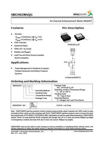
SM3402NSQG N-Channel Enhancement Mode MOSFET Features Pin Description D D D 30V/50A, D RDS(ON) =4.6m (max.) @ VGS =10V RDS(ON) =6.2m (max.) @ VGS =4.5V SG S S ESD Protected DFN3x3D-8_EP Avalanche Rated 100% UIS + Rg Tested (5,6,7,8) DDDD Reliable and Rugged Lead Free and Green Devices Available (RoHS Compliant) (4) G Applications Power Management in Noteb
9.8. Size:152K sino
sm3401nsqg.pdf 

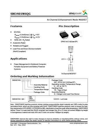
SM3401NSQG N-Channel Enhancement Mode MOSFET Features Pin Description D D D 30V/50A, D RDS(ON) =2.8m (max.) @ VGS =10V RDS(ON) =3.6m (max.) @ VGS =4.5V G S S S 100% UIS + Rg Tested DFN3.3x3.3-8(Saw-EP) Avalanche Rated Reliable and Rugged (5,6,7,8) D D DD Lead Free and Green Devices Available (RoHS Compliant) Applications (4) G Power Management in Notebook Com
9.9. Size:248K sino
sm3407psqa.pdf 

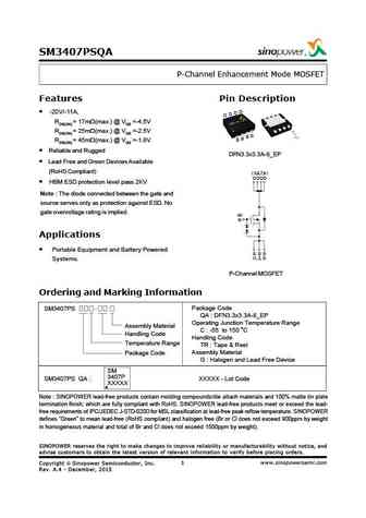
SM3407PSQA P-Channel Enhancement Mode MOSFET Features Pin Description D -20V/-11A, D D D RDS(ON) = 17m (max.) @ VGS =-4.5V RDS(ON) = 25m (max.) @ VGS =-2.5V G S S RDS(ON) = 45m (max.) @ VGS =-1.8V S Reliable and Rugged DFN3.3x3.3A-8_EP Lead Free and Green Devices Available (RoHS Compliant) ( 5,6,7,8 ) DDDD HBM ESD protection level pass 2KV Note The diode connected
9.10. Size:148K sino
sm3408nsqg.pdf 

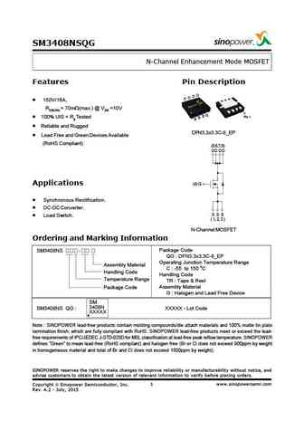
SM3408NSQG N-Channel Enhancement Mode MOSFET Features Pin Description D D D D 150V/16A, RDS(ON) = 70m (max.) @ VGS =10V G S Pin 1 100% UIS + Rg Tested S S Reliable and Rugged DFN3.3x3.3C-8_EP Lead Free and Green Devices Available (RoHS Compliant) (5,6,7,8) DDDD Applications (4) G Synchronous Rectification. DC-DC Converter. S S S Load Switch. ( 1, 2, 3 )
9.11. Size:891K globaltech semi
gsm3400.pdf 

GSM3400 GSM3400 30V N-Channel Enhancement Mode MOSFET Product Description Features GSM3400, N-Channel enhancement mode 30V/4.0A,RDS(ON)=48m @VGS=10V MOSFET, uses Advanced Trench 30V/3.5A,RDS(ON)=52m @VGS=4.5V Technology to provide excellent RDS(ON), low 30V/2.8A,RDS(ON)=58m @VGS=2.5V gate charge. These devices are particularly Super high density cell des
9.12. Size:867K globaltech semi
gsm3404.pdf 

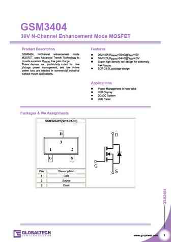
GSM3404 30V N-Channel Enhancement Mode MOSFET Product Description Features GSM3404, N-Channel enhancement mode 30V/4.0A,RDS(ON)=30m @VGS=10V MOSFET, uses Advanced Trench Technology to 30V/3.2A,RDS(ON)=34m @VGS=4.5V provide excellent RDS(ON) ,low gate charge. Super high density cell design for extremely These devices are particularly suited for low low RDS (ON) Volta
9.13. Size:898K globaltech semi
gsm3403a.pdf 

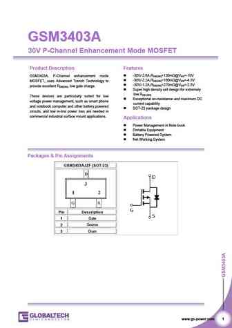
GSM3403A GSM3403A 30V P-Channel Enhancement Mode MOSFET Product Description Features -30V/-2.6A,RDS(ON)=130m @VGS=-10V GSM3403A, P-Channel enhancement mode -30V/-2.2A,RDS(ON)=160m @VGS=-4.5V MOSFET, uses Advanced Trench Technology to -30V/-1.2A,RDS(ON)=270m @VGS=-2.5V provide excellent RDS(ON), low gate charge. Super high density cell design for extremel
9.14. Size:453K globaltech semi
gsm3402a.pdf 

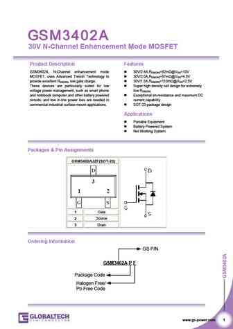
30V N-Channel Enhancement Mode MOSFET Product Description Features GSM3402A, N-Channel enhancement mode 30V/2.4A,RDS(ON)=82m @VGS=10V MOSFET, uses Advanced Trench Technology to 30V/2.0A,RDS(ON)=87m @VGS=4.5V provide excellent RDS(ON), low gate charge. 30V/1.5A,RDS(ON)=110m @VGS=2.5V These devices are particularly suited for low Super high density cell design for
9.15. Size:922K globaltech semi
gsm3400a.pdf 

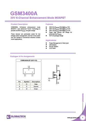
GSM3400A 30V N-Channel Enhancement Mode MOSFET Product Description Features GSM3400A, N-Channel enhancement mode 30V/2.4A,RDS(ON)=54m @VGS=10V MOSFET, uses Advanced Trench Technology to 30V/1.8A,RDS(ON)=58m @VGS=4.5V provide excellent RDS(ON), low gate charge. 30V/1.5A,RDS(ON)=65m @VGS=2.5V Super high density cell design for These devices are particularly suited for lo
9.16. Size:885K globaltech semi
gsm3406s.pdf 

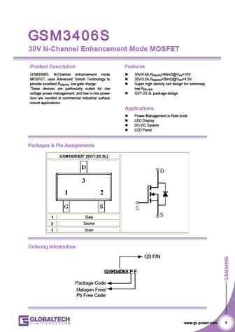
30V N-Channel Enhancement Mode MOSFET Product Description Features GSM3406S, N-Channel enhancement mode 30V/4.0A,RDS(ON)=40m @VGS=10V MOSFET, uses Advanced Trench Technology to 30V/3.5A,RDS(ON)=50m @VGS=4.5V provide excellent RDS(ON), low gate charge. Super high density cell design for extremely These devices are particularly suited for low low RDS (ON) voltage power
9.17. Size:864K globaltech semi
gsm3407s.pdf 

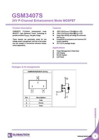
GSM3407S 30V P-Channel Enhancement Mode MOSFET Product Description Features GSM3407S, P-Channel enhancement mode -30V/-3.6A,RDS(ON)=75m @VGS=-10V MOSFET, uses Advanced Trench Technology to -30V/-3.2A,RDS(ON)=95m @VGS=-4.5V provide excellent RDS(ON), low gate charge. Super high density cell design for extremely low RDS (ON) These devices are particularly suited for
9.18. Size:884K globaltech semi
gsm3406.pdf 

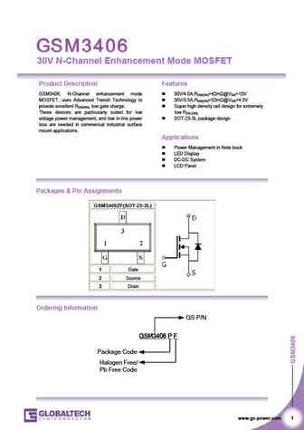
30V N-Channel Enhancement Mode MOSFET Product Description Features GSM3406, N-Channel enhancement mode 30V/4.0A,RDS(ON)=42m @VGS=10V MOSFET, uses Advanced Trench Technology to 30V/3.5A,RDS(ON)=52m @VGS=4.5V provide excellent RDS(ON), low gate charge. Super high density cell design for extremely These devices are particularly suited for low low RDS (ON) voltage power
9.19. Size:846K globaltech semi
gsm3407as.pdf 

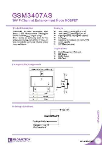
30V P-Channel Enhancement Mode MOSFET Product Description Features GSM3407AS, P-Channel enhancement mode -30V/-2.8A,RDS(ON)=77m @VGS=-10.0V MOSFET, uses Advanced Trench Technology to -30V/-2.4A,RDS(ON)=102m @VGS=-4.5V provide excellent RDS(ON), low gate charge. Super high density cell design for extremely These devices are particularly suited for low low RDS (ON)
9.20. Size:1144K globaltech semi
gsm3402.pdf 

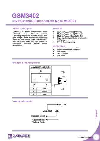
GSM3402 GSM3402 30V N-Channel Enhancement Mode MOSFET Product Description Features GSM3402, N-Channel enhancement mode 30V/4.0A,RDS(ON)=75m @VGS=10V MOSFET, uses Advanced Trench 30V/3.5A,RDS(ON)=80m @VGS=4.5V Technology to provide excellent RDS(ON), low 30V/2.8A,RDS(ON)=100m @VGS=2.5V gate charge. These devices are particularly Super high density cell de
9.21. Size:863K globaltech semi
gsm3406a.pdf 

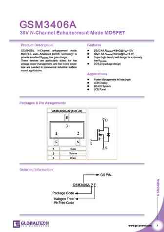
30V N-Channel Enhancement Mode MOSFET Product Description Features GSM3406A, N-Channel enhancement mode 30V/2.4A,RDS(ON)=48m @VGS=10V MOSFET, uses Advanced Trench Technology to 30V/1.8A,RDS(ON)=58m @VGS=4.5V provide excellent RDS(ON), low gate charge. Super high density cell design for extremely These devices are particularly suited for low low RDS (ON) voltage power
9.22. Size:1426K globaltech semi
gsm3401s.pdf 

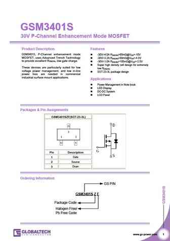
GSM3401S GSM3401S 30V P-Channel Enhancement Mode MOSFET Product Description Features GSM3401S, P-Channel enhancement mode -30V/-4.0A RDS(ON)=65m @VGS=-10V MOSFET, uses Advanced Trench Technology -30V/-3.2A RDS(ON)=80m @VGS=-4.5V to provide excellent RDS(ON), low gate charge. -30V/-1.0A RDS(ON)=105m @VGS=-2.5V Super high density cell design for extremely These devi
9.23. Size:898K globaltech semi
gsm3403.pdf 

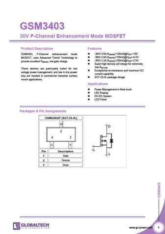
GSM3403 GSM3403 30V P-Channel Enhancement Mode MOSFET Product Description Features -30V/-3.0A,RDS(ON)=125m @VGS=-10V GSM3403, P-Channel enhancement mode -30V/-2.6A,RDS(ON)=155m @VGS=-4.5V MOSFET, uses Advanced Trench Technology to -30V/-1.2A,RDS(ON)=220m @VGS=-2.5V provide excellent RDS(ON), low gate charge. Super high density cell design for extremely
9.24. Size:452K globaltech semi
gsm3400as.pdf 

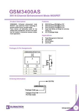
30V N-Channel Enhancement Mode MOSFET Product Description Features GSM3400AS, N-Channel enhancement mode 30V/2.8A,RDS(ON)=50m @VGS=10V MOSFET, uses Advanced Trench Technology to 30V/2.5A,RDS(ON)=55m @VGS=4.5V provide excellent RDS(ON), low gate charge. 30V/2.2A,RDS(ON)=75m @VGS=2.5V These devices are particularly suited for low Super high density cell design for
9.25. Size:877K globaltech semi
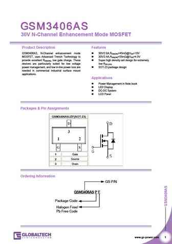
gsm3406as.pdf 

30V N-Channel Enhancement Mode MOSFET Product Description Features GSM3406AS, N-Channel enhancement mode 30V/2.8A,RDS(ON)=45m @VGS=10V MOSFET, uses Advanced Trench Technology to 30V/2.4A,RDS(ON)=55m @VGS=4.5V provide excellent RDS(ON), low gate charge. These Super high density cell design for extremely devices are particularly suited for low voltage low RDS (ON) powe
9.26. Size:612K globaltech semi
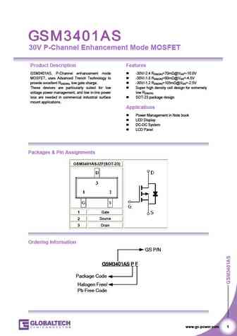
gsm3401as.pdf 

30V P-Channel Enhancement Mode MOSFET Product Description Features GSM3401AS, P-Channel enhancement mode -30V/-2.4 RDS(ON)=70m @VGS=-10.0V MOSFET, uses Advanced Trench Technology to -30V/-1.8 RDS(ON)=80m @VGS=-4.5V provide excellent RDS(ON), low gate charge. -30V/-1.2 RDS(ON)=105m @VGS=-2.5V These devices are particularly suited for low Super high density cell de
9.27. Size:921K globaltech semi
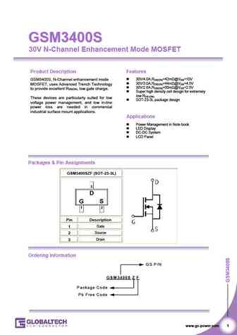
gsm3400s.pdf 

GSM3400S GSM3400S 30V N-Channel Enhancement Mode MOSFET Product Description Features 30V/4.0A,RDS(ON)=42m @VGS=10V GSM3400S, N-Channel enhancement mode 30V/3.0A,RDS(ON)=44m @VGS=4.5V MOSFET, uses Advanced Trench Technology 30V/2.6A,RDS(ON)=50m @VGS=2.5V to provide excellent RDS(ON), low gate charge. Super high density cell design for extremely low RDS (ON) The
9.28. Size:605K jsmsemi
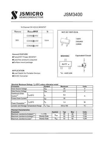
jsm3400.pdf 

JSM3400 N-Channel 30-V(D-S) MOSFET V(BR)DSS RDS(on)MAX ID SOT-23 SOT-23-3L / 0.028 @ 10V 3 1.GATE 30V 5.8A 0.033 @ 4.5V 2.SOURCE 3.DRAIN 1 0.052 @ 2.5V 2 General FEATURE Equivalent Circuit MARKING TrenchFET Power MOSFET Lead free product is acquired Surface mount package A01TF w APPLICATION *w week code Load Switch for Portable Devices DC/DC Convert
9.29. Size:546K jsmsemi
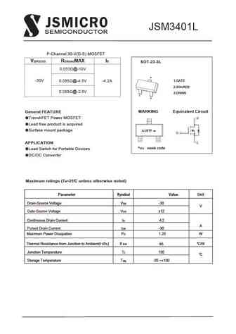
jsm3401l.pdf 

JSM3401L P-Channel 30-V(D-S) MOSFET V(BR)DSS RDS(on)MAX ID SOT-23-3L 0.053 @-10V 3 -30V 0.065 @-4.5V 1.GATE -4.2A 2.SOURCE 0.085 @-2.5V 3.DRAIN 1 2 MARKING Equivalent Circuit General FEATURE TrenchFET Power MOSFET Lead free product is acquired Surface mount package A19TF w APPLICATION *w week code Load Switch for Portable Devices DC/DC Converter Maximu
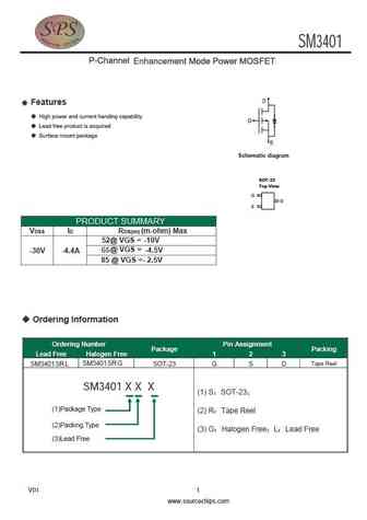
9.30. Size:9601K cn sps
sm3401.pdf 

SM3401 Features Schematic diagram SOT-23 Top View G D S PRODUCT SUMMARY VDSS ID RDS(on) (m-ohm) Max 52@ VGS = -10V 65@ VGS = -4.5V -30V -4.4A 85 @ VGS =- 2.5V Ordering Information Ordering Number Pin Assignment Package Packing Lead Free Halogen Free 1 2 3 SM3401SR G SM3401SR L SOT-23 G S D Tape Reel SM3401 X X X (1) S SOT-23 (1)Packa
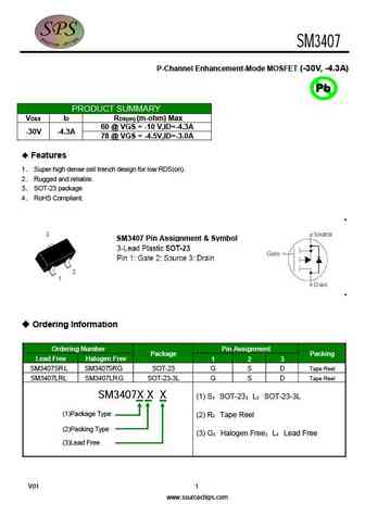
9.31. Size:3541K cn sps
sm3407.pdf 

SM3407 P-Channel Enhancement-Mode MOSFET (-30V, -4.3A) Pb PRODUCT SUMMARY VDSS ID RDS(on) (m-ohm) Max 60 @ VGS = -10 V,ID=-4.3A -30V -4.3A 78 @ VGS = -4.5V,ID=-3.0A Features 1 Super high dense cell trench design for low RDS(on). 2 Rugged and reliable. 3 SOT-23 package 4 RoHS Compliant. SM3407 Pin Assignment & Symbol Ordering Information
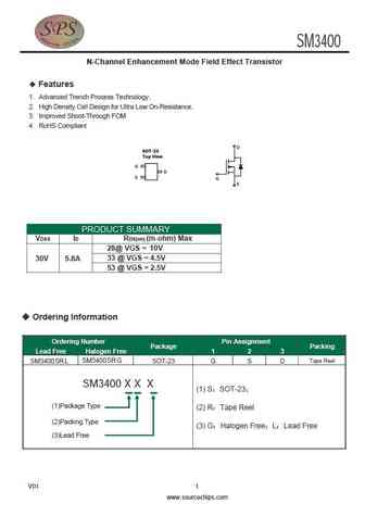
9.32. Size:4431K cn sps
sm3400.pdf 

SM3400 N-Channel Enhancement Mode Field Effect Transistor P-Channel Enhancement-Mode MOSFET Features 1 Advanced Trench Process Technology. 2 High Density Cell Design for Ultra Low On-Resistance. 3 Improved Shoot-Through FOM 4 RoHS Compliant D SOT-23 Top View G D S G S PRODUCT SUMMARY VDSS ID RDS(on) (m-ohm) Max 28@ VGS = 10V 33 @ VGS = 4.5V 30V 5.8A
9.33. Size:771K cn sps
sm3402srl.pdf 

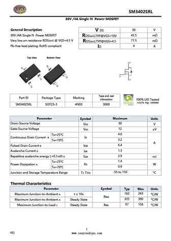
SM3402SRL 30V /4A Single N Power MOSFET B N03B N 30V /4A Single N Power MOSFET 4N03B General Description 30 V V DS 30V /4A Single N Power MOSFET 45.5 m RDS(on),TYP@VGS=10V Very low on-resistance RDS(on) @ VGS=4.5 V 71.5 m RDS(on),TYP@VGS=4.5 Pb-free lead plating; RoHS compliant 4 A ID Tape and reel Part ID Package Type Marking infomation 100% UIS Tested 100% Rg Tested SM340
9.34. Size:765K cn sps
sm3404srl.pdf 

SM3404SRL 30V /5A Single N Power MOSFET B N03B N 30V /5A Single N Power MOSFET 5N03B General Description 30 V V DS 30V /5A Single N Power MOSFET 30.1 m RDS(on),TYP@VGS=10V Very low on-resistance RDS(on) @ VGS=4.5 V 47.3 m RDS(on),TYP@VGS=4.5 Pb-free lead plating; RoHS compliant 5 A ID Tape and reel Part ID Package Type Marking infomation 100% UIS Tested 100% Rg Tested SM340
Otros transistores... SM4023NSU
, SM4024NSK
, SM4024NSKP
, SM4024NSU
, SM4026NSUC
, SM4028NSU
, SM3402NSQG
, SM3404NSQG
, NCEP15T14
, SM3406NSQG
, SM3408NSQG
, SM3412NHQG
, SM3424NHQA
, SM3425NHQA
, SM3433NHQG
, SM3439NHQA
, SM6128NSK
.


