AOD4158P Datasheet. Equivalente. Reemplazo. Hoja de especificaciones. Principales características
Número de Parte: AOD4158P
Tipo de FET: MOSFET
Polaridad de transistor: N
ESPECIFICACIONES MÁXIMAS
Pdⓘ - Máxima disipación de potencia: 32 W
|Vds|ⓘ - Voltaje máximo drenador-fuente: 30 V
|Vgs|ⓘ - Voltaje máximo fuente-puerta: 20 V
|Id|ⓘ - Corriente continua de drenaje: 46 A
Tjⓘ - Temperatura máxima de unión: 175 °C
CARACTERÍSTICAS ELÉCTRICAS
trⓘ - Tiempo de subida: 14.7 nS
Cossⓘ - Capacitancia de salida: 500 pF
RDSonⓘ - Resistencia estado encendido drenaje a fuente: 0.009 Ohm
Encapsulados: TO-252
Búsqueda de reemplazo de AOD4158P MOSFET
- Selecciónⓘ de transistores por parámetros
AOD4158P datasheet
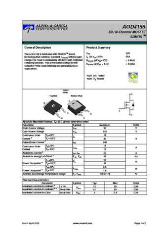
aod4156.pdf

isc N-Channel MOSFET Transistor AOD4156 FEATURES Drain Current I = 55A@ T =25 D C Drain Source Voltage- V =30V(Min) DSS Static Drain-Source On-Resistance R =5.6m (Max) DS(on) 100% avalanche tested Minimum Lot-to-Lot variations for robust device performance and reliable operation DESCRIPTION Designed for use in switch mode power supplies and general purpose
aod4146.pdf
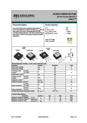
AOD4146/AOI4146 30V N-Channel MOSFET TM SDMOS General Description Product Summary 30V The AOD4146/AOI4146 is fabricated with SDMOSTM VDS ID (at VGS=10V) 55A trench technology that combines excellent RDS(ON) with low gate charge.The result is outstanding efficiency with RDS(ON) (at VGS=10V)
aod4191l.pdf
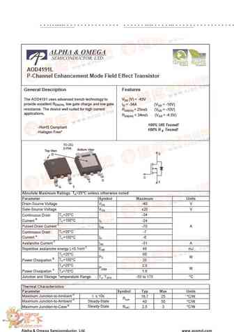
AOD4191L PCB 24 AOD4191L P-Channel Enhancement Mode Field Effect Transistor General Description Features The AOD4191 uses advanced trench technology to VDS (V) = -40V provide excellent RDS(ON), low gate charge and low gate ID = -34A (VGS = -10V) resistance. The device well suited for high current RDS(ON)
aod4185 aoi4185.pdf

AOD4185/AOI4185 P-Channel Enhancement Mode Field Effect Transistor General Description Features The AOD4185/AOI4185 uses advanced trench VDS (V) = -40V technology to provide excellent RDS(ON) and low gate ID = -40A (VGS = -10V) charge. With the excellent thermal resistance of the RDS(ON)
aod417.pdf
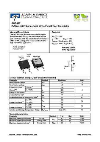
AOD417 P-Channel Enhancement Mode Field Effect Transistor General Description Features The AOD417 uses advanced trench technology to provide excellent RDS(ON), low gate charge and low VDS (V) = -30V gate resistance. With the excellent thermal resistance ID = -25A (VGS = -10V) of the DPAK package, this device is well suited for RDS(ON)
aod4130 aoi4130.pdf
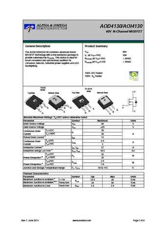
AOD4130/AOI4130 60V N-Channel MOSFET General Description Product Summary VDS 60V The AOD4130/AOI4130 combines advanced trench MOSFET technology with a low resistance package to ID (at VGS=10V) 30A provide extremely low RDS(ON). This device is ideal for RDS(ON) (at VGS=10V)
aod4189.pdf
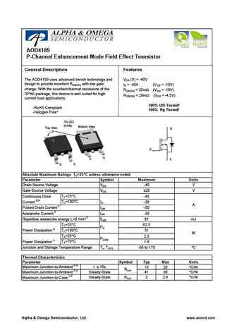
AOD4189 P-Channel Enhancement Mode Field Effect Transistor General Description Features The AOD4189 uses advanced trench technology and VDS (V) = -40V design to provide excellent RDS(ON) with low gate ID = -40A (VGS = -10V) charge. With the excellent thermal resistance of the RDS(ON)
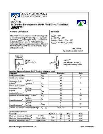
aod410.pdf
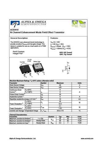
AOD410 N-Channel Enhancement Mode Field Effect Transistor General Description Features The AOD410 uses advanced trench technology to VDS (V) = 30V provide excellent RDS(ON) and low gate charge. This ID = 8A (VGS = 10V) device is suitable for use as a load switch or in PWM RDS(ON)
aod4126.pdf

AOD4126/AOI4126 100V N-Channel MOSFET TM SDMOS General Description Product Summary 100V The AOD4126&AOI4126 are fabricated with SDMOSTM VDS ID (at VGS=10V) 43A trench technology that combines excellent RDS(ON) with low gate charge.The result is outstanding efficiency with RDS(ON) (at VGS=10V)
aod413a.pdf
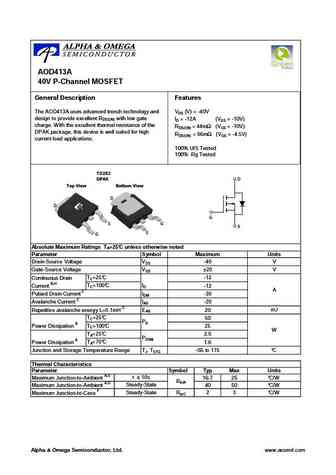
AOD413A 40V P-Channel MOSFET General Description Features The AOD413A uses advanced trench technology and VDS (V) = -40V design to provide excellent RDS(ON) with low gate ID = -12A (VGS = -10V) charge. With the excellent thermal resistance of the RDS(ON)
aod4102.pdf
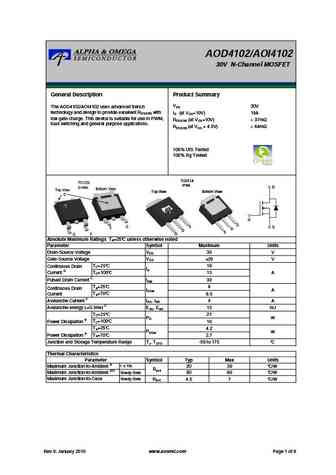
AOD4102/AOI4102 30V N-Channel MOSFET General Description Product Summary VDS 30V The AOD4102/AOI4102 uses advanced trench technology and design to provide excellent RDS(ON) with ID (at VGS=10V) 19A low gate charge. This device is suitable for use in PWM, RDS(ON) (at VGS=10V)
aod4128.pdf
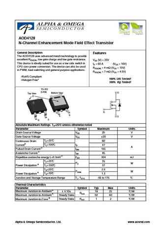
AOD4128 N-Channel Enhancement Mode Field Effect Transistor General Description Features The AOD4128 uses advanced trench technology to provide excellent RDS(ON), low gate charge and low gate resistance. VDS (V) = 25V This device is ideally suited for use as a low side switch in ID = 60 A (VGS = 10V) CPU core power conversion. The device can also be used RDS(ON)
aod4185.pdf

AOD4185/AOI4185 P-Channel Enhancement Mode Field Effect Transistor General Description Features The AOD4185/AOI4185 uses advanced trench VDS (V) = -40V technology to provide excellent RDS(ON) and low gate ID = -40A (VGS = -10V) charge. With the excellent thermal resistance of the RDS(ON)
aod4144.pdf
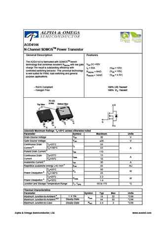
AOD4144 N-Channel SDMOSTM Power Transistor General Description Features The AOD4144 is fabricated with SDMOSTM trench VDS (V) =30V technology that combines excellent RDS(ON) with low gate charge.The result is outstanding efficiency with (VGS = 10V) ID = 55A controlled switching behavior. This universal technology (VGS = 10V) RDS(ON)
aod4184.pdf
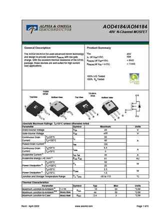
AOD4184/AOI4184 40V N-Channel MOSFET General Description Product Summary VDS The AOD4184/AOI4184 used advanced trench technology 40V 50A and design to provide excellent RDS(ON) with low gate ID (at VGS=10V) charge. With the excellent thermal resistance of the DPAK
aod4132.pdf
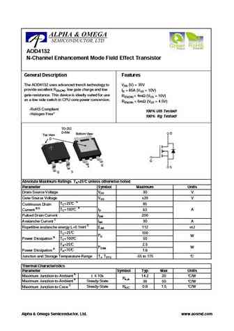
AOD4132 N-Channel Enhancement Mode Field Effect Transistor General Description Features The AOD4132 uses advanced trench technology to VDS (V) = 30V provide excellent RDS(ON), low gate charge and low ID = 85A (VGS = 10V) gate resistance. This device is ideally suited for use RDS(ON)
aod4124.pdf
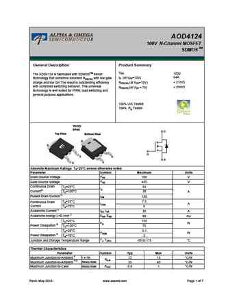
AOD4124 100V N-Channel MOSFET TM SDMOS General Description Product Summary VDS 100V The AOD4124 is fabricated with SDMOSTM trench 54A ID (at VGS=10V) technology that combines excellent RDS(ON) with low gate
aod4187.pdf
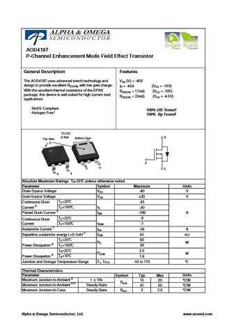
AOD4187 P-Channel Enhancement Mode Field Effect Transistor General Description Features The AOD4187 uses advanced trench technology and VDS (V) = -40V design to provide excellent RDS(ON) with low gate charge. ID = -45A (VGS = -10V) With the excellent thermal resistance of the DPAK RDS(ON)
aod4184a.pdf
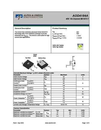
AOD4184A 40V N-Channel MOSFET General Description Product Summary VDS The AOD4184A combines advanced trench MOSFET 40V 50A technology with a low resistance package to provide ID (at VGS=10V) extremely low RDS(ON). This device is well suited for high
aod4182.pdf
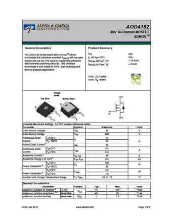
AOD4182 80V N-Channel MOSFET TM SDMOS General Description Product Summary VDS 80V The AOD4182 is fabricated with SDMOSTM trench ID (at VGS=10V) 53A technology that combines excellent RDS(ON) with low gate
aod4180.pdf

AOD4180 80V N-Channel MOSFET TM SDMOS General Description Product Summary VDS 80V The AOD4180 is fabricated with SDMOSTM trench 54A ID (at VGS=10V) technology that combines excellent RDS(ON) with low gate
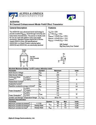
aod4100.pdf
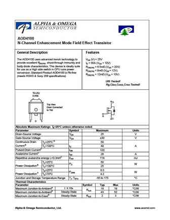
AOD4100 N-Channel Enhancement Mode Field Effect Transistor General Description Features The AOD4100 uses advanced trench technology to VDS (V) = 25V provide excellent RDS(ON), shoot-through immunity and ID = 50A (VGS = 10V) body diode characteristics. This device is ideally suite RDS(ON)
aod414.pdf
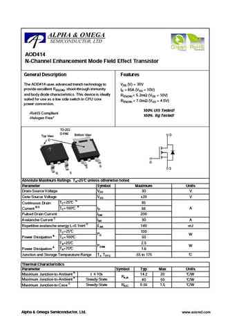
AOD414 N-Channel Enhancement Mode Field Effect Transistor General Description Features The AOD414 uses advanced trench technology to VDS (V) = 30V provide excellent RDS(ON), shoot-through immunity ID = 85A (VGS = 10V) and body diode characteristics. This device is ideally RDS(ON)
aod4120.pdf
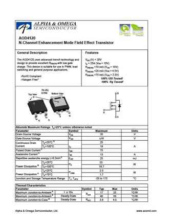
AOD4120 N-Channel Enhancement Mode Field Effect Transistor 1.4 General Description Features The AOD4120 uses advanced trench technology and VDS (V) = 20V design to provide excellent RDS(ON) with low gate ID = 25A (VGS = 10V) charge. This device is suitable for use in PWM, load RDS(ON)
aod4136.pdf
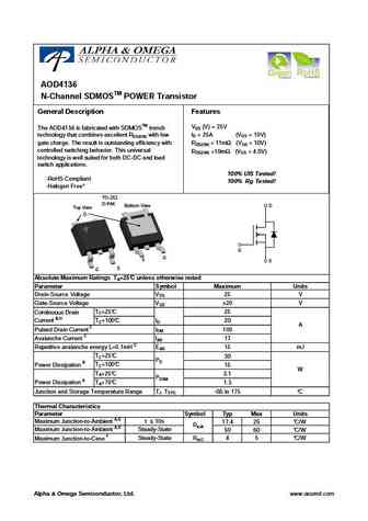
AOD4136 N-Channel SDMOSTM POWER Transistor General Description Features VDS (V) = 25V The AOD4136 is fabricated with SDMOSTM trench ID = 25A (VGS = 10V) technology that combines excellent RDS(ON) with low gate charge. The result is outstanding efficiency with RDS(ON)
aod4130.pdf

AOD4130/AOI4130 60V N-Channel MOSFET General Description Product Summary VDS 60V The AOD4130/AOI4130 combines advanced trench MOSFET technology with a low resistance package to ID (at VGS=10V) 30A provide extremely low RDS(ON). This device is ideal for RDS(ON) (at VGS=10V)
aod4186.pdf
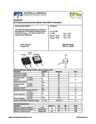
AOD4186 N-Channel Enhancement Mode Field Effect Transistor General Description Features The AOD4186 combines advanced trench MOSFET technology with a low resistance package to provide VDS (V) =40V extremely low RDS(ON). This device is ideal for low (VGS = 10V) ID = 35A voltage inverter applications. (VGS = 10V) RDS(ON)
aod4104.pdf
AOD4104 N-Channel Enhancement Mode Field Effect Transistor General Description Features The AOD4104 uses advanced trench technology to VDS (V) = 25V provide excellent RDS(ON), shoot-through immunity and ID = 75A (VGS = 10V) body diode characteristics. This device is ideally suite RDS(ON)
aod4106.pdf
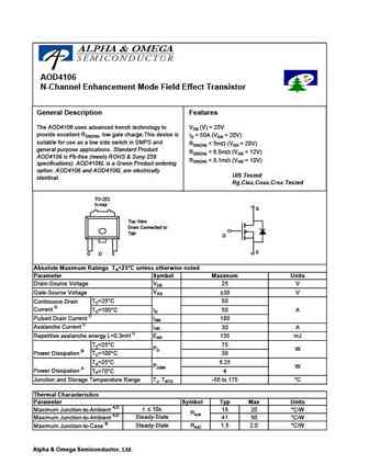
AOD4106 N-Channel Enhancement Mode Field Effect Transistor General Description Features The AOD4106 uses advanced trench technology to VDS (V) = 25V provide excellent RDS(ON), low gate charge.This device is ID = 50A (VGS = 20V) suitable for use as a low side switch in SMPS and RDS(ON)
aod4126 aoi4126.pdf
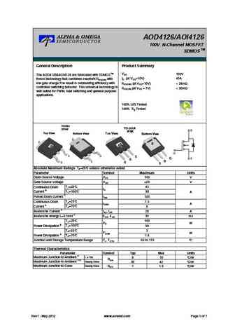
AOD4126/AOI4126 100V N-Channel MOSFET TM SDMOS General Description Product Summary 100V The AOD4126&AOI4126 are fabricated with SDMOSTM VDS ID (at VGS=10V) 43A trench technology that combines excellent RDS(ON) with low gate charge.The result is outstanding efficiency with RDS(ON) (at VGS=10V)
aod4184 aoi4184.pdf

AOD4184/AOI4184 40V N-Channel MOSFET General Description Product Summary VDS 40V The AOD4184/AOI4184 used advanced trench technology and design to provide excellent RDS(ON) with ID (at VGS=10V) 50A low gate charge. With the excellent thermal resistance of RDS(ON) (at VGS=10V)
aod418.pdf
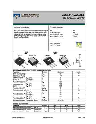
AOD418/AOI418 30V N-Channel MOSFET General Description Product Summary VDS The AOD418/AOI418 uses advanced trench technology to 30V 36A provide excellent RDS(ON), low gate charge and low gate ID (at VGS= 10V) resistance. With the excellent thermal resistance of the
aod4112.pdf
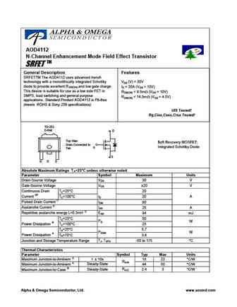
AOD4112 N-Channel Enhancement Mode Field Effect Transistor SRFET TM General Description Features SRFETTM The AOD4112 uses advanced trench technology with a monolithically integrated Schottky VDS (V) = 30V diode to provide excellent R ,and low gate charge. ID = 20A (VGS = 10V) DS(ON) This device is suitable for use as a low side FET in RDS(ON)
aob413 aod413.pdf
AOB413/AOD413 30A 40V P-channel Enhancement Mode Power MOSFET 1 Description These P-channel enhanced vdmosfets, used advanced V = -40V DSS trench technology and design, provide to excellent Rdson with low gate charge. Which accords with the R = 30m DS(on) (TYP) RoHS standard. I = -30A D 2 Features Fast switching Low on resistance Low gate charge Low reverse tr
aod413.pdf
SMD Type MOSFET P-Channel MOSFET AOD413 (KOD413) TO-252 Unit mm 6.50+0.15 -0.15 +0.1 2.30 -0.1 +0.2 5.30-0.2 +0.8 0.50 -0.7 Features 4 VDS (V) =-40V ID =-12 A (VGS =-10V) RDS(ON) 45m (VGS =-10V) 0.127 0.80+0.1 max -0.1 RDS(ON) 69m (VGS =-4.5V) 1 Gate 2 Drain 2.3 0.60+ 0.1 - 0.1 3 Source +0.15 4.60 -0.15 4 Drain D G S Absol
aod417.pdf
AOD417 www.VBsemi.tw P-Channel 30-V (D-S) MOSFET FEATURES PRODUCT SUMMARY Halogen-free According to IEC 61249-2-21 VDS (V) RDS(on) ( ) ID (A)d Qg (Typ.) Definition 0.018 at VGS = - 10 V - 40 TrenchFET Power MOSFET - 30 13 nC 100 % Rg Tested 0.025 at VGS = - 4.5 V - 35 APPLICATIONS Load Switch Battery Switch S TO-252 G D G D S P-Channel MOSFET ABSO
aod4189.pdf
AOD4189 www.VBsemi.tw P-Channel 4 0 V (D-S) MOSFET FEATURES PRODUCT SUMMARY TrenchFET power MOSFET VDS (V) -40 Package with low thermal resistance RDS(on) ( ) at VGS = -10 V 0.012 100 % Rg and UIS tested RDS(on) ( ) at VGS = -4.5 V 0.015 ID (A) -50 Configuration Single TO-252 S G D D G S P-Channel MOSFET Top View ABSOLUTE MAXIMUM RATINGS (TC = 25 C, unle
aod410.pdf
AOD410 www.VBsemi.tw N-Channel 30-V (D-S) MOSFET FEATURES PRODUCT SUMMARY TrenchFET Power MOSFET VDS (V) RDS(on) ( ) ID (A)a, e Qg (Typ) 100 % Rg and UIS Tested Compliant to RoHS Directive 2011/65/EU 0.007 at VGS = 10 V 50 30 25 nC 0.009 at VGS = 4.5 V 40 APPLICATIONS D OR-ing Server TO-252 DC/DC G G D S S Top View N-Channel MOSFET ABSOLUT
aod4185.pdf

AOD4185 www.VBsemi.tw P-Channel 4 0 V (D-S) MOSFET FEATURES PRODUCT SUMMARY TrenchFET power MOSFET VDS (V) -40 Package with low thermal resistance RDS(on) ( ) at VGS = -10 V 0.012 100 % Rg and UIS tested RDS(on) ( ) at VGS = -4.5 V 0.015 ID (A) -50 Configuration Single TO-252 S G D D G S P-Channel MOSFET Top View ABSOLUTE MAXIMUM RATINGS (TC = 25 C, unle
aod4144.pdf

AOD4144 www.VBsemi.tw N-Channel 30-V (D-S) MOSFET FEATURES PRODUCT SUMMARY TrenchFET Power MOSFET VDS (V) RDS(on) ( ) ID (A)a, e Qg (Typ) 100 % Rg and UIS Tested Compliant to RoHS Directive 2011/65/EU 0.005 at VGS = 10 V 80 30 31 nC 0.006 at VGS = 4.5 V 68 APPLICATIONS D OR-ing TO-252 Server DC/DC G G D S Top View S N-Channel MOSFET ABSOLUT
aod4184.pdf
AOD4184 www.VBsemi.tw N-Channel 40-V (D-S) MOSFET FEATURES PRODUCT SUMMARY TrenchFET Power MOSFET VDS (V) RDS(on) ( ) ID (A)a, c Qg (Typ.) 100 % Rg and UIS Tested RoHS 0.0050 at VGS = 10 V 85 COMPLIANT 40 80 nC 0.0065 at VGS = 4.5 V 70 APPLICATIONS Synchronous Rectification Power Supplies D TO-252 G G D S S N-Channel MOSFET ABSOLUTE MAXIMUM RATI
aod4132.pdf

AOD4132 www.VBsemi.tw N-Channel 30-V (D-S) MOSFET FEATURES PRODUCT SUMMARY TrenchFET Power MOSFET VDS (V) RDS(on) ( ) ID (A)a, e Qg (Typ) 100 % Rg and UIS Tested Compliant to RoHS Directive 2011/65/EU 0.002 at VGS = 10 V 100 30 72 nC 0.003 at VGS = 4.5 V 90 APPLICATIONS D OR-ing Server TO-252 DC/DC G G D S Top View S N-Channel MOSFET ABSOL
aod4180.pdf
AOD4180 www.VBsemi.tw N-Channel 80 V (D-S) MOSFET FEATURES PRODUCT SUMMARY TrenchFET Power MOSFET VDS (V) RDS(on) ( ) Max. ID (A) Qg (Typ.) 100 % Rg and UIS Tested 0.0055 at VGS = 10 V 75a 80 0.0088 at VGS = 6.0 V 65a 17.1 nC APPLICATIONS 0.0115 at VGS = 5.0 V 54 Primary Side Switching Synchronous Rectification TO-252 D DC/AC Inverters LED Backlightin
aod414.pdf
AOD414 www.VBsemi.tw N-Channel 30-V (D-S) MOSFET FEATURES PRODUCT SUMMARY TrenchFET Power MOSFET VDS (V) RDS(on) ( ) ID (A)a, e Qg (Typ) 100 % Rg and UIS Tested Compliant to RoHS Directive 2011/65/EU 0.002 at VGS = 10 V 100 30 72 nC 0.003 at VGS = 4.5 V 90 APPLICATIONS D OR-ing Server TO-252 DC/DC G G D S Top View S N-Channel MOSFET ABSOLU
aod4130.pdf
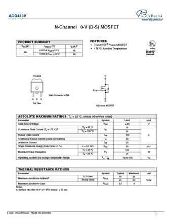
AOD4130 www.VBsemi.tw N-Channel 6 0-V (D-S) MOSFET FEATURES PRODUCT SUMMARY TrenchFET Power MOSFET VDS (V) rDS(on) ( ) ID (A)a Available 175 C Junction Temperature 0.025 at VGS = 10 V 35 RoHS* 60 0.030 at VGS = 4.5 V 30 COMPLIANT TO-252 D G Drain Connected to Tab G D S S Top View N-Channel MOSFET ABSOLUTE MAXIMUM RATINGS TC = 25 C, unless otherwise noted
aod4112.pdf

AOD4112 www.VBsemi.tw N-Channel 30-V (D-S) MOSFET FEATURES PRODUCT SUMMARY TrenchFET Power MOSFET VDS (V) RDS(on) ( ) ID (A)a, e Qg (Typ) 100 % Rg and UIS Tested Compliant to RoHS Directive 2011/65/EU 0.007 at VGS = 10 V 50 30 25 nC 0.009 at VGS = 4.5 V 40 APPLICATIONS D OR-ing Server TO-252 DC/DC G G D S S Top View N-Channel MOSFET ABSOLU
aod4146.pdf

isc N-Channel MOSFET Transistor AOD4146 FEATURES Drain Current I = 55A@ T =25 D C Drain Source Voltage- V =30V(Min) DSS Static Drain-Source On-Resistance R =5.6m (Max) DS(on) 100% avalanche tested Minimum Lot-to-Lot variations for robust device performance and reliable operation DESCRIPTION Designed for use in switch mode power supplies and general purpose
aod417.pdf

isc P-Channel MOSFET Transistor AOD417 FEATURES Drain Current I =-25A@ T =25 D C Drain Source Voltage- V =-30V(Min) DSS Static Drain-Source On-Resistance R = 34m (Max) DS(on) 100% avalanche tested Minimum Lot-to-Lot variations for robust device performance and reliable operation DESCRIPTION Designed for use in switch mode power supplies and general purpose
aod4189.pdf

isc P-Channel MOSFET Transistor AOD4189 FEATURES Drain Current I = -40A@ T =25 D C Drain Source Voltage- V =-40V(Min) DSS Static Drain-Source On-Resistance R =22m (Max) DS(on) 100% avalanche tested Minimum Lot-to-Lot variations for robust device performance and reliable operation DESCRIPTION Designed for use in switch mode power supplies and general purpose
aod4126.pdf

isc N-Channel MOSFET Transistor AOD4126 FEATURES Drain Current I = 43A@ T =25 D C Drain Source Voltage- V =100V(Min) DSS Static Drain-Source On-Resistance R =24m (Max) DS(on) 100% avalanche tested Minimum Lot-to-Lot variations for robust device performance and reliable operation DESCRIPTION Designed for use in switch mode power supplies and general purpose
aod413a.pdf

isc P-Channel MOSFET Transistor AOD413A FEATURES Drain Current I = -12A@ T =25 D C Drain Source Voltage- V =-40V(Min) DSS Static Drain-Source On-Resistance R =11m (Max) DS(on) 100% avalanche tested Minimum Lot-to-Lot variations for robust device performance and reliable operation DESCRIPTION Designed for use in switch mode power supplies and general purpose
aod4102.pdf

isc N-Channel MOSFET Transistor AOD4102 FEATURES Drain Current I = 19A@ T =25 D C Drain Source Voltage- V =30V(Min) DSS Static Drain-Source On-Resistance R =37m (Max) DS(on) 100% avalanche tested Minimum Lot-to-Lot variations for robust device performance and reliable operation DESCRIPTION Designed for use in switch mode power supplies and general purpose a
aod4128.pdf
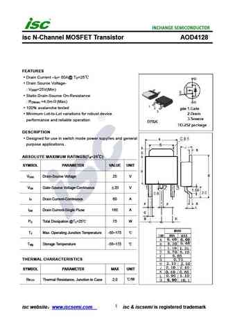
isc N-Channel MOSFET Transistor AOD4128 FEATURES Drain Current I = 60A@ T =25 D C Drain Source Voltage- V =25V(Min) DSS Static Drain-Source On-Resistance R =4.0m (Max) DS(on) 100% avalanche tested Minimum Lot-to-Lot variations for robust device performance and reliable operation DESCRIPTION Designed for use in switch mode power supplies and general purpose
aod4185.pdf
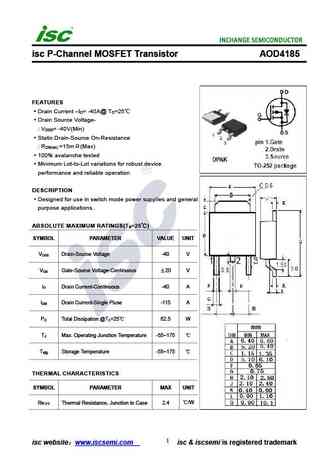
isc P-Channel MOSFET Transistor AOD4185 FEATURES Drain Current I = -40A@ T =25 D C Drain Source Voltage- V = -40V(Min) DSS Static Drain-Source On-Resistance R =15m (Max) DS(on) 100% avalanche tested Minimum Lot-to-Lot variations for robust device performance and reliable operation DESCRIPTION Designed for use in switch mode power supplies and general purpos
aod4184.pdf
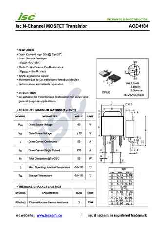
isc N-Channel MOSFET Transistor AOD4184 FEATURES Drain Current I = 50A@ T =25 D C Drain Source Voltage- V = 40V(Min) DSS Static Drain-Source On-Resistance R = 8m (Max) DS(on) 100% avalanche tested Minimum Lot-to-Lot variations for robust device performance and reliable operation DESCRITION Be suitable for synchronous rectification for server and general
aod4132.pdf

isc N-Channel MOSFET Transistor AOD4132 FEATURES Drain Current I = 85A@ T =25 D C Drain Source Voltage- V =30V(Min) DSS Static Drain-Source On-Resistance R =4.0m (Max) DS(on) 100% avalanche tested Minimum Lot-to-Lot variations for robust device performance and reliable operation DESCRIPTION Designed for use in switch mode power supplies and general purpose
aod4124.pdf
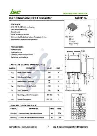
INCHANGE Semiconductor isc N-Channel MOSFET Transistor AOD4124 FEATURES With TO-252(DPAK) packaging High speed switching Easy to use 100% avalanche tested Minimum Lot-to-Lot variations for robust device performance and reliable operation APPLICATIONS Power supply Load switching General purpose applications Switching applications ABSOLUTE MAXIMUM RATINGS(T =
aod4184a.pdf

isc N-Channel MOSFET Transistor AOD4184A FEATURES Drain Current I = 50A@ T =25 D C Drain Source Voltage- V = 40V(Min) DSS Static Drain-Source On-Resistance R = 7m (Max) DS(on) 100% avalanche tested Minimum Lot-to-Lot variations for robust device performance and reliable operation DESCRITION Be suitable for synchronous rectification for server and genera
aod4182.pdf

isc N-Channel MOSFET Transistor AOD4182 FEATURES Drain Current I = 53A@ T =25 D C Drain Source Voltage- V =80V(Min) DSS Static Drain-Source On-Resistance R =15.5m (Max) DS(on) 100% avalanche tested Minimum Lot-to-Lot variations for robust device performance and reliable operation DESCRIPTION Designed for use in switch mode power supplies and general purpose
aod4180.pdf

isc N-Channel MOSFET Transistor AOD4180 FEATURES Drain Current I = 54A@ T =25 D C Drain Source Voltage- V =80V(Min) DSS Static Drain-Source On-Resistance R =14m (Max) DS(on) 100% avalanche tested Minimum Lot-to-Lot variations for robust device performance and reliable operation DESCRIPTION Designed for use in switch mode power supplies and general purpose a
aod4120.pdf

isc N-Channel MOSFET Transistor AOD4120 FEATURES Drain Current I = 25A@ T =25 D C Drain Source Voltage- V =20V(Min) DSS Static Drain-Source On-Resistance R =18m (Max) DS(on) 100% avalanche tested Minimum Lot-to-Lot variations for robust device performance and reliable operation DESCRIPTION Designed for use in switch mode power supplies and general purpose a
aod4136.pdf

isc N-Channel MOSFET Transistor AOD4136 FEATURES Drain Current I = 25A@ T =25 D C Drain Source Voltage- V =25V(Min) DSS Static Drain-Source On-Resistance R =11m (Max) DS(on) 100% avalanche tested Minimum Lot-to-Lot variations for robust device performance and reliable operation DESCRIPTION Designed for use in switch mode power supplies and general purpose a
aod4130.pdf
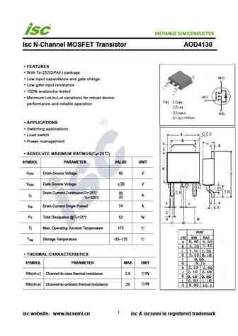
INCHANGE Semiconductor Isc N-Channel MOSFET Transistor AOD4130 FEATURES With To-252(DPAK) package Low input capacitance and gate charge Low gate input resistance 100% avalanche tested Minimum Lot-to-Lot variations for robust device performance and reliable operation APPLICATIONS Switching applications Load switch Power management ABSOLUTE MAXIMUM RATINGS(T =25
aod4186.pdf
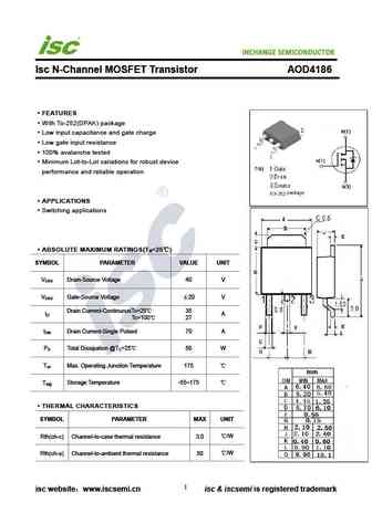
INCHANGE Semiconductor Isc N-Channel MOSFET Transistor AOD4186 FEATURES With To-252(DPAK) package Low input capacitance and gate charge Low gate input resistance 100% avalanche tested Minimum Lot-to-Lot variations for robust device performance and reliable operation APPLICATIONS Switching applications ABSOLUTE MAXIMUM RATINGS(T =25 ) a SYMBOL PARAMETER VALUE UNI
aod418.pdf
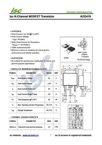
isc N-Channel MOSFET Transistor AOD418 FEATURES Drain Current I = 36A@ T =25 D C Drain Source Voltage- V = 30V(Min) DSS Static Drain-Source On-Resistance R = 7.5m (Max) DS(on) 100% avalanche tested Minimum Lot-to-Lot variations for robust device performance and reliable operation DESCRITION Be suitable for synchronous rectification for server and genera
Otros transistores... AOD661, AOD294A, AOD296A, AOD2146, AOD2610E, AOD2904, AOD2910E, AOD66406, TK10A60D, AOE6930, AOE6932, AOE6936, AOH3254, AOI294A, AOI296A, AOI2606, AOI2610
History: SIHF9Z22 | SFF27N50M
🌐 : EN ES РУ

Liste
Recientemente añadidas las descripciónes de los transistores:
MOSFET: ASDM7002EZA | ASDM68N80KQ | ASDM6802ZC | ASDM60R042NQ | ASDM60P12KQ | ASDM60N80KQ | ASDM60N70Q | ASDM60N50KQ | ASDM60N45KQ | ASDM60N30KQ | ASDM540G | ASDM4976S | ASDM4606S | ASDM40R009NQ | ASDM40N80KQ | ASDM40N60KQ
Popular searches
2n5087 | ksa1381 | bc546 | 2sc458 | a733 transistor | mpsa92 | tip142 | d882