IRFS610A MOSFET Equivalente. Reemplazo. Hoja de especificaciones. Principales características
Número de Parte: IRFS610A
Tipo de FET: MOSFET
Polaridad de transistor: N
ESPECIFICACIONES MÁXIMAS
Pdⓘ - Máxima
disipación de potencia: 22 W
|Vds|ⓘ - Voltaje máximo drenador-fuente: 200 V
|Vgs|ⓘ - Voltaje máximo fuente-puerta: 30 V
|Id|ⓘ - Corriente continua
de drenaje: 2.5 A
Tjⓘ - Temperatura máxima de unión: 150 °C
CARACTERÍSTICAS ELÉCTRICAS
trⓘ - Tiempo
de subida: 10 nS
Cossⓘ - Capacitancia de salida: 35 pF
RDSonⓘ - Resistencia estado encendido drenaje a fuente: 1.5 Ohm
Encapsulados: TO220F
Búsqueda de reemplazo de IRFS610A MOSFET
- Selecciónⓘ de transistores por parámetros
IRFS610A datasheet
..1. Size:261K 1
irfs610a.pdf 
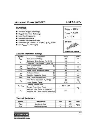
IRFS610A Advanced Power MOSFET FEATURES BVDSS = 200 V Avalanche Rugged Technology RDS(on) = 1.5 Rugged Gate Oxide Technology Lower Input Capacitance ID = 2.5 A Improved Gate Charge Extended Safe Operating Area TO-220F Lower Leakage Current 10 A (Max.) @ VDS = 200V Low RDS(ON) 1.169 (Typ.) 1 2 3 1.Gate 2. Drain 3. Source Absolute Maximum Ratings Symbol Ch
8.2. Size:853K fairchild semi
irfs614b.pdf

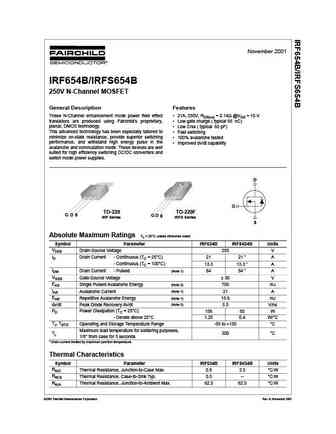
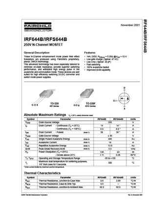
November 2001 IRF614B/IRFS614B 250V N-Channel MOSFET General Description Features These N-Channel enhancement mode power field effect 2.8A, 250V, RDS(on) = 2.0 @VGS = 10 V transistors are produced using Fairchild s proprietary, Low gate charge ( typical 8.1 nC) planar, DMOS technology. Low Crss ( typical 7.5 pF) This advanced technology has been especially tailored to
9.5. Size:875K 1
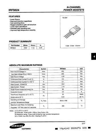
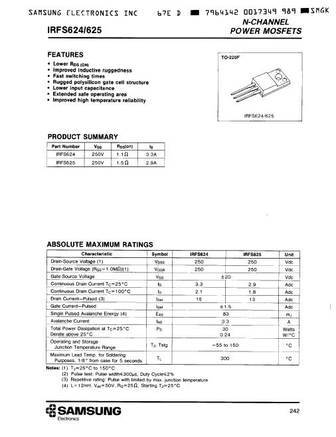
irfs624b irf624b.pdf

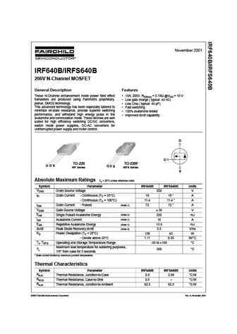
November 2001 IRF624B/IRFS624B 250V N-Channel MOSFET General Description Features These N-Channel enhancement mode power field effect 4.1A, 250V, RDS(on) = 1.1 @VGS = 10 V transistors are produced using Fairchild s proprietary, Low gate charge ( typical 13.5 nC) planar, DMOS technology. Low Crss ( typical 9.5 pF) This advanced technology has been especially tailored to
9.7. Size:261K 1
irfs650a.pdf

IRFS650A Advanced Power MOSFET FEATURES BVDSS = 200 V Avalanche Rugged Technology RDS(on) = 0.085 Rugged Gate Oxide Technology Lower Input Capacitance ID = 15.8 A Improved Gate Charge Extended Safe Operating Area TO-220F Lower Leakage Current 10 A (Max.) @ VDS = 200V Low RDS(ON) 0.071 (Typ.) 1 2 3 1.Gate 2. Drain 3. Source Absolute Maximum Ratings Sym
9.14. Size:859K 1
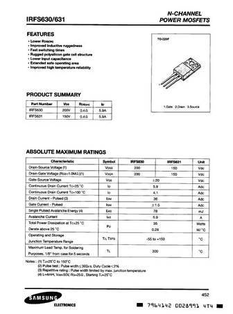
irf630b irfs630b.pdf
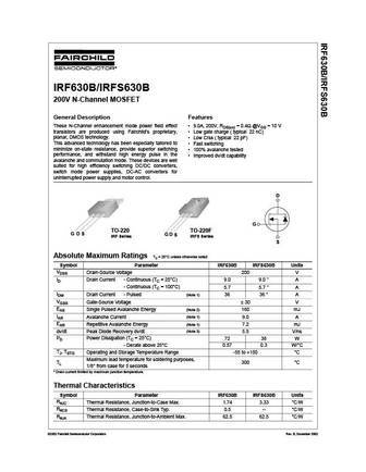
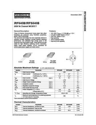
IRF630B/IRFS630B 200V N-Channel MOSFET General Description Features These N-Channel enhancement mode power field effect 9.0A, 200V, RDS(on) = 0.4 @VGS = 10 V transistors are produced using Fairchild s proprietary, Low gate charge ( typical 22 nC) planar, DMOS technology. Low Crss ( typical 22 pF) This advanced technology has been especially tailored to Fast switchin
9.15. Size:266K international rectifier
auirfs6535 auirfsl6535.pdf
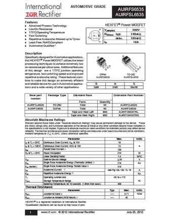
AUTOMOTIVE GRADE AUIRFS6535 AUIRFSL6535 Features HEXFET Power MOSFET Advanced Process Technology D Low On-Resistance V(BR)DSS 300V 175 C Operating Temperature RDS(on) typ. 148m Fast Switching G max. 185m Repetitive Avalanche Allowed up to Tjmax S ID 19A Lead-Free, RoHS Compliant Automotive Qualified * Description D Specifically designed
9.18. Size:874K fairchild semi
irf624b irfs624b.pdf

November 2001 IRF624B/IRFS624B 250V N-Channel MOSFET General Description Features These N-Channel enhancement mode power field effect 4.1A, 250V, RDS(on) = 1.1 @VGS = 10 V transistors are produced using Fairchild s proprietary, Low gate charge ( typical 13.5 nC) planar, DMOS technology. Low Crss ( typical 9.5 pF) This advanced technology has been especially tailored to
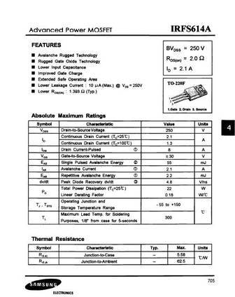
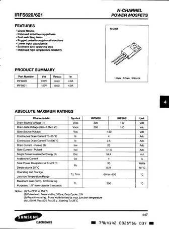
9.24. Size:508K samsung
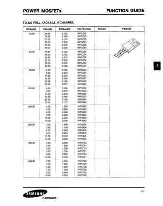
irfs630a.pdf

Advanced Power MOSFET FEATURES BVDSS = 200 V Avalanche Rugged Technology RDS(on) = 0.4 Rugged Gate Oxide Technology Lower Input Capacitance ID = 6.5 A Improved Gate Charge Extended Safe Operating Area Lower Leakage Current 10 A (Max.) @ VDS = 200V Low RDS(ON) 0.333 (Typ.) 1 2 3 1.Gate 2. Drain 3. Source Absolute Maximum Ratings Symbol Characteristic Valu
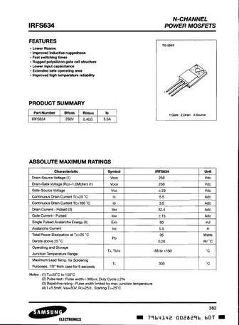
9.25. Size:504K samsung
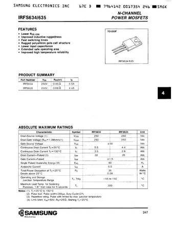
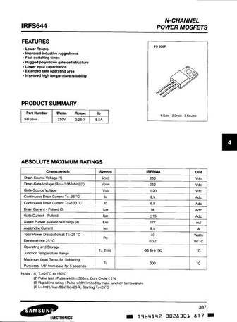
irfs644a.pdf

Advanced Power MOSFET FEATURES BVDSS = 250 V Avalanche Rugged Technology RDS(on) = 0.28 Rugged Gate Oxide Technology Lower Input Capacitance ID = 7.9 A Improved Gate Charge Extended Safe Operating Area Lower Leakage Current 10 A (Max.) @ VDS = 250V Lower RDS(ON) 0.214 (Typ.) 1 2 3 1.Gate 2. Drain 3. Source Absolute Maximum Ratings Symbol Characteristic V
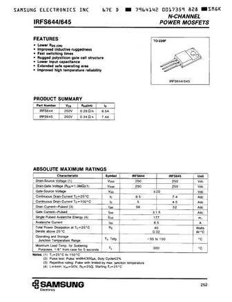
9.26. Size:505K samsung
irfs634a.pdf
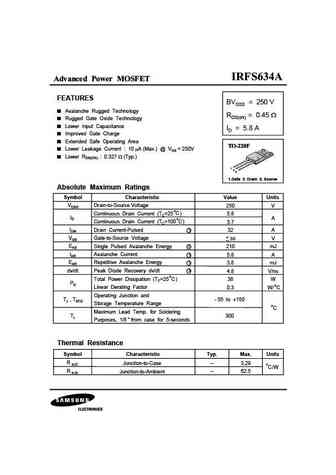
Advanced Power MOSFET FEATURES BVDSS = 250 V Avalanche Rugged Technology RDS(on) = 0.45 Rugged Gate Oxide Technology Lower Input Capacitance ID = 5.8 A Improved Gate Charge Extended Safe Operating Area Lower Leakage Current 10 A (Max.) @ VDS = 250V Lower RDS(ON) 0.327 (Typ.) 1 2 3 1.Gate 2. Drain 3. Source Absolute Maximum Ratings Symbol Characteristic V
9.27. Size:511K samsung
irfs624a.pdf

Advanced Power MOSFET FEATURES BVDSS = 250 V Avalanche Rugged Technology RDS(on) = 1.1 Rugged Gate Oxide Technology Lower Input Capacitance ID = 3.4 A Improved Gate Charge Extended Safe Operating Area Lower Leakage Current 10 A (Max.) @ VDS = 250V Low RDS(ON) 0.742 (Typ.) 1 2 3 1.Gate 2. Drain 3. Source Absolute Maximum Ratings Symbol Characteristic Valu
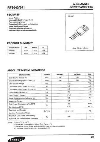
9.28. Size:508K samsung
irfs640a.pdf

Advanced Power MOSFET FEATURES BVDSS = 200 V Avalanche Rugged Technology RDS(on) = 0.18 Rugged Gate Oxide Technology Lower Input Capacitance ID = 9.8 A Improved Gate Charge Extended Safe Operating Area Lower Leakage Current 10 A (Max.) @ VDS = 200V Lower RDS(ON) 0.144 (Typ. ) 1 2 3 1.Gate 2. Drain 3. Source Absolute Maximum Ratings Symbol Characteristic
9.30. Size:515K samsung
irfs654a.pdf

Advanced Power MOSFET FEATURES BVDSS = 250 V Avalanche Rugged Technology RDS(on) = 0.14 Rugged Gate Oxide Technology Lower Input Capacitance ID = 12 A Improved Gate Charge Extended Safe Operating Area Lower Leakage Current 10 A (Max.) @ VDS = 250V Low RDS(ON) 0.108 (Typ.) 1 2 3 1.Gate 2. Drain 3. Source Absolute Maximum Ratings Symbol Characteristic Valu
9.31. Size:701K infineon
auirfs6535 auirfsl6535.pdf
AUTOMOTIVE GRADE AUIRFS6535 AUIRFSL6535 HEXFET Power MOSFET Features Advanced Process Technology VDSS 300V Low On-Resistance RDS(on) typ. 148m 175 C Operating Temperature Fast Switching max. 185m Repetitive Avalanche Allowed up to Tjmax ID 19A Lead-Free, RoHS Compliant Automotive Qualified * D D Description Specific
Otros transistores... IRFS532, IRFS533, IRFS540, IRFS540A, IRFS541, IRFS542, IRFS543, IRFS550A, SKD502T, IRFS614A, IRFS620, IRFS620A, IRFS622, IRFS624, IRFS624A, IRFS625, IRFS630