MTB300N10L3 Datasheet. Equivalente. Reemplazo. Hoja de especificaciones. Principales características
Número de Parte: MTB300N10L3 📄📄
Tipo de FET: MOSFET
Polaridad de transistor: N
ESPECIFICACIONES MÁXIMAS
Pdⓘ - Máxima disipación de potencia: 3.1 W
|Vds|ⓘ - Voltaje máximo drenador-fuente: 100 V
|Vgs|ⓘ - Voltaje máximo fuente-puerta: 20 V
|Id|ⓘ - Corriente continua de drenaje: 1.9 A
Tjⓘ - Temperatura máxima de unión: 150 °C
CARACTERÍSTICAS ELÉCTRICAS
trⓘ - Tiempo de subida: 16.2 nS
Cossⓘ - Capacitancia de salida: 21 pF
RDSonⓘ - Resistencia estado encendido drenaje a fuente: 0.365 Ohm
Encapsulados: SOT-223
📄📄 Copiar
Búsqueda de reemplazo de MTB300N10L3 MOSFET
- Selecciónⓘ de transistores por parámetros
MTB300N10L3 datasheet
mtb300n10l3.pdf
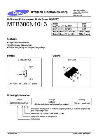
Spec. No. C580L3 Issued Date 2014.12.24 CYStech Electronics Corp. Revised Date Page No. 1/9 N-Channel Enhancement Mode Power MOSFET BVDSS 100V MTB300N10L3 ID@VGS=10V, TA=25 C 1.9A ID@VGS=10V, TC=25 C 5.0A RDSON@VGS=10V, ID=2.9A 290m (typ) RDSON@VGS=5V, ID=2.9A 302m (typ) Features Single Drive Requirement Fast Switching Characteristic Pb-free
mtb30n06vlrev4.pdf
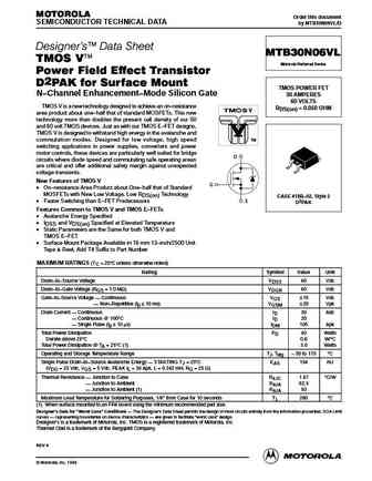
MOTOROLA Order this document SEMICONDUCTOR TECHNICAL DATA by MTB30N06VL/D Designer's Data Sheet MTB30N06VL TMOS V Motorola Preferred Device Power Field Effect Transistor D2PAK for Surface Mount TMOS POWER FET N Channel Enhancement Mode Silicon Gate 30 AMPERES 60 VOLTS TMOS V is a new technology designed to achieve an on resistance RDS(on) = 0.050 OHM area product abou
mtb30p06v.pdf
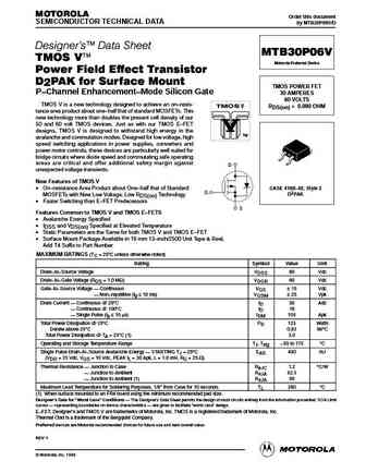
MOTOROLA Order this document SEMICONDUCTOR TECHNICAL DATA by MTB30P06V/D Designer's Data Sheet MTB30P06V TMOS V Motorola Preferred Device Power Field Effect Transistor D2PAK for Surface Mount TMOS POWER FET P Channel Enhancement Mode Silicon Gate 30 AMPERES 60 VOLTS TMOS V is a new technology designed to achieve an on resis- RDS(on) = 0.080 OHM tance area product abou
mtb30p06vrev1x.pdf

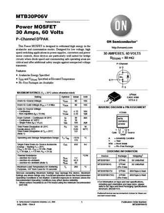
MOTOROLA Order this document SEMICONDUCTOR TECHNICAL DATA by MTB30P06V/D Designer's Data Sheet MTB30P06V TMOS V Motorola Preferred Device Power Field Effect Transistor D2PAK for Surface Mount TMOS POWER FET P Channel Enhancement Mode Silicon Gate 30 AMPERES 60 VOLTS TMOS V is a new technology designed to achieve an on resis- RDS(on) = 0.080 OHM tance area product abou


Otros transistores... MTB110P10L3, MTB160N25J3, MTB20A06Q8, MTB20N04J3, MTB23P06VT4, MTB25C04Q8, MTB2D5N03BH8, MTB2P50ET4G, IRFB4110, MTB30P06VT4, MTB30P06VT4G, MTB3D0N03BH8, MTB50P03HDLG, MTB50P03HDLT4, MTB50P03HDLT4G, MTB5D0P03J3, MTB5D0P03Q8
History: 2SK3633 | AP10G04S | WSR25N20 | MSF20N50 | AP1605 | MSW16N50 | SI5481DU
🌐 : EN ES РУ

Liste
Recientemente añadidas las descripciónes de los transistores:
MOSFET: BCD70N07A | BCD90N03 | BCD80N06 | T50N06 | H50N06 | BCD12N65 | BCT12N65 | BCD4N65 | BCT4N65 | BCD7N65 | BCT7N65 | BCT20N65 | ASDM30P100KQ | ASDM30N90Q | ASDM30N75KQ | ASDM30N150Q
Popular searches
c5200 2sc5200 transistor datasheet | d2390 datasheet | 2sa750 replacement | 2sc984 replacement | a1046 transistor | hy19p03 | 2sk2749 | c2577 transistor