IRFW614A MOSFET Equivalente. Reemplazo. Hoja de especificaciones. Principales características
Número de Parte: IRFW614A
Tipo de FET: MOSFET
Polaridad de transistor: N
ESPECIFICACIONES MÁXIMAS
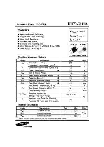
Pdⓘ - Máxima disipación de potencia: 40 W
|Vds|ⓘ - Voltaje máximo drenador-fuente: 250 V
|Vgs|ⓘ - Voltaje máximo fuente-puerta: 30 V
|Id|ⓘ - Corriente continua de drenaje: 2.8 A
Tjⓘ - Temperatura máxima de unión: 150 °C
CARACTERÍSTICAS ELÉCTRICAS
trⓘ - Tiempo de subida: 11 nS
Cossⓘ - Capacitancia de salida: 35 pF
RDSonⓘ - Resistencia estado encendido drenaje a fuente: 2 Ohm
Encapsulados: TO263
Búsqueda de reemplazo de IRFW614A MOSFET
- Selecciónⓘ de transistores por parámetros
IRFW614A datasheet
irfw614a.pdf
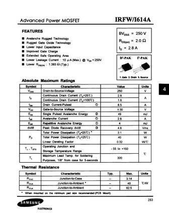
Advanced Power MOSFET FEATURES BVDSS = 250 V Avalanche Rugged Technology RDS(on) = 2.0 Rugged Gate Oxide Technology Lower Input Capacitance ID = 2.8 A Improved Gate Charge Extended Safe Operating Area Lower Leakage Current 10 A (Max.) @ VDS = 250V 2 Lower RDS(ON) 1.393 (Typ.) 1 1 2 3 3 1. Gate 2. Drain 3. Source Absolute Maximum Ratings Symbol Cha
irfw610b irfi610b.pdf
November 2001 IRFW610B / IRFI610B 200V N-Channel MOSFET General Description Features These N-Channel enhancement mode power field effect 3.3A, 200V, RDS(on) = 1.5 @VGS = 10 V transistors are produced using Fairchild s proprietary, Low gate charge ( typical 7.2 nC) planar, DMOS technology. Low Crss ( typical 6.8 pF) This advanced technology has been especially tailored t

Otros transistores... IRFUC20 , IRFW450 , IRFW510A , IRFW520A , IRFW530A , IRFW540A , IRFW550A , IRFW610A , IRFP250N , IRFW620A , IRFW624A , IRFW630A , IRFW634A , IRFW640A , IRFW644A , IRFW710A , IRFW720A .
🌐 : EN ES РУ

Liste
Recientemente añadidas las descripciónes de los transistores:
MOSFET: ASD80R750E | ASD70R950E | ASD70R600E | ASD70R380E | ASD65R850E | ASD65R550E | ASD65R350E | ASD65R300E | ASD65R280E | ASD65R270E | ASD60R330E | ASD60R280E | ASB80R750E | ASB70R380E | ASB65R300E | ASB65R220E
Popular searches
a933 | 2sa818 replacement | irfb3607 datasheet | 2n2907 equivalent | c2026 | mpsa56 transistor equivalent | 13009 transistor | irf3205 equivalent