SD2100 MOSFET Equivalente. Reemplazo. Hoja de especificaciones. Principales características
Número de Parte: SD2100
Tipo de FET: MOSFET
Polaridad de transistor: N
ESPECIFICACIONES MÁXIMAS
Pdⓘ - Máxima
disipación de potencia: 0.3 W
|Vds|ⓘ - Voltaje máximo drenador-fuente: 25 V
|Vgs|ⓘ - Voltaje máximo fuente-puerta: 25 V
|Id|ⓘ - Corriente continua
de drenaje: 0.05 A
Tjⓘ - Temperatura máxima de unión: 150 °C
CARACTERÍSTICAS ELÉCTRICAS
trⓘ - Tiempo
de subida: 0.4 nS
RDSonⓘ - Resistencia estado encendido drenaje a fuente: 50 Ohm
Encapsulados: TO-72
Búsqueda de reemplazo de SD2100 MOSFET
- Selecciónⓘ de transistores por parámetros
SD2100 datasheet
..1. Size:26K calogic
sd2100.pdf 
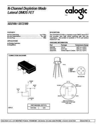
N-Channel Depletion Mode Lateral DMOS FET LLC SD2100 / SST2100 FEATURES DESCRIPTION ON Fast Switching . . . . . . . . . . . . . . . . . . . . . . . . . t 1.0ns The SD2100/SST2100 is a depletion mode DMOS lateral FET rss Low Capacitance . . . . . . . . . . . . . . . . . . . . . . . . . c 2pf that provides ultra high speed switching with very low Low R . . . . . . .
0.1. Size:144K sanyo
2sd2100.pdf
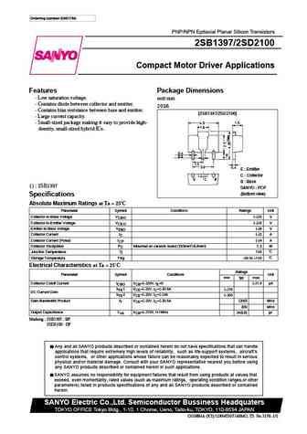
Ordering number EN3176A PNP/NPN Epitaxial Planar Silicon Transistors 2SB1397/2SD2100 Compact Motor Driver Applications Features Package Dimensions Low saturation voltage. unit mm Contains diode between collector and emitter. 2038 Contains bias resistance between base and emitter. [2SB1397/2SD2100] Large current capacity. Small-sized package making it easy to prov
0.2. Size:1046K kexin
2sd2100.pdf
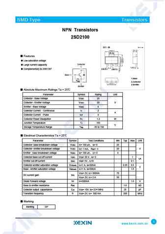
SMD Type Transistors NPN Transistors 2SD2100 1.70 0.1 Features Low saturation voltage Collector Large current cappacity 0.42 0.1 Complementary to 2SB1397 0.46 0.1 Base 1.Base RBE 2.Collector 3.Emitter Emitter Absolute Maximum Ratings Ta = 25 Parameter Symbol Rating Unit Collector - Base Voltage VCBO 25 Collector - Emitter Voltage VCEO 20 V Emitt
9.2. Size:353K samsung
ssd2104.pdf

8 SOIC FEATURES 1 8 S D S 2 7 D 3 6 S D Lower RDS(ON) 4 5 G D Improved Inductive Ruggedness Top View Fast Swtching Times S S S Low Input Capacitance Extended Safe Operating Area Improved High Temperature Reliability G Product Summary Part Number BVdss Rds(on) ID D D D D SSD2104 - 30V 0.07 - 4.6A P-Channel MOSFET Absolute Maximu
9.3. Size:363K samsung
ssd2101.pdf
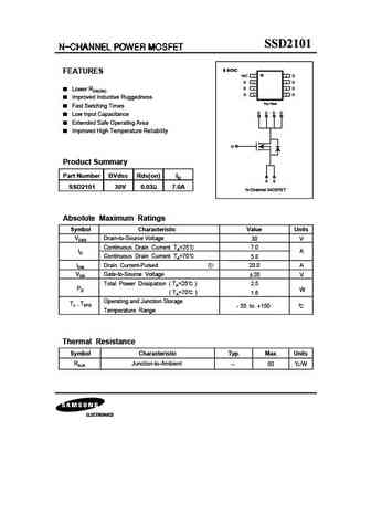
8 SOIC FEATURES 1 8 N/C D S 2 7 D 3 6 S D Lower RDS(ON) 4 5 G D Improved Inductive Ruggedness Top View Fast Swtching Times D D D D Low Input Capacitance Extended Safe Operating Area Improved High Temperature Reliability G Product Summary Part Number BVdss Rds(on) ID S S SSD2101 30V 0.03 7.0A N-Channel MOSFET Absolute Maximum Ratings S
9.4. Size:242K samsung
ssd2106.pdf
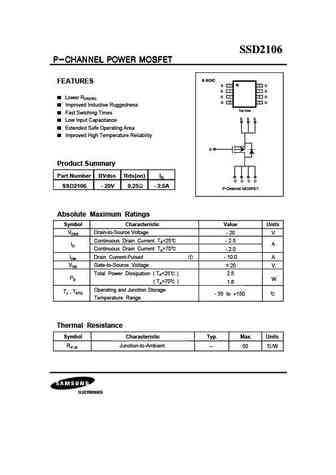
8 SOIC FEATURES 1 8 S D S 2 7 D 3 6 S D Lower RDS(ON) 4 5 G D Improved Inductive Ruggedness Top View Fast Swtching Times S S S Low Input Capacitance Extended Safe Operating Area Improved High Temperature Reliability G Product Summary Part Number BVdss Rds(on) ID D D D D SSD2106 - 20V 0.25 - 2.5A P-Channel MOSFET Absolute Maximu
9.5. Size:361K samsung
ssd2108.pdf

8 SOIC FEATURES 1 8 S D S 2 7 D 3 6 S D Lower RDS(ON) 4 5 G D Improved Inductive Ruggedness Top View Fast Swtching Times S S S Low Input Capacitance Extended Safe Operating Area Improved High Temperature Reliability G Product Summary Part Number BVdss Rds(on) ID D D D D SSD2108 - 20V 0.10 - 4.3A P-Channel MOSFET Absolute Maximu
9.6. Size:353K samsung
ssd2102.pdf

8 SOIC FEATURES 1 8 S D S 2 7 D 3 6 S D Lower RDS(ON) 4 5 G D Improved Inductive Ruggedness Top View Fast Swtching Times S S S Low Input Capacitance Extended Safe Operating Area Improved High Temperature Reliability G Product Summary Part Number BVdss Rds(on) ID D D D D SSD2102 - 20V 0.06 - 5.3A P-Channel MOSFET Absolute Maximu
9.7. Size:35K hitachi
2sd2104.pdf
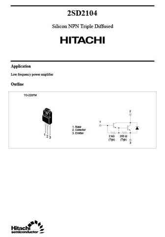
2SD2104 Silicon NPN Triple Diffused Application Low frequency power amplifier Outline TO-220FM 2 1 1. Base 2. Collector 3. Emitter 1 2 k 200 2 3 (Typ) (Typ) 3 2SD2104 Absolute Maximum Ratings (Ta = 25 C) Item Symbol Rating Unit Collector to base voltage VCBO 120 V Collector to emitter voltage VCEO 120 V Emitter to base voltage VEBO 7V Collector current IC 8A Col
9.8. Size:35K hitachi
2sd2106.pdf
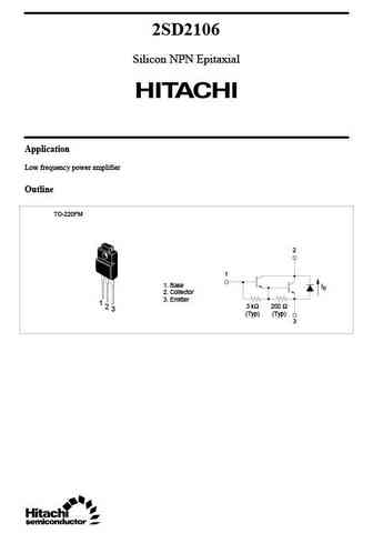
2SD2106 Silicon NPN Epitaxial Application Low frequency power amplifier Outline TO-220FM 2 1 1. Base ID 2. Collector 3. Emitter 1 3 k 200 2 3 (Typ) (Typ) 3 2SD2106 Absolute Maximum Ratings (Ta = 25 C) Item Symbol Rating Unit Collector to base voltage VCBO 120 V Collector to emitter voltage VCEO 120 V Emitter to base voltage VEBO 7V Collector current IC 6A Colle
9.9. Size:351K hitachi
2sd2108.pdf
2SD2108 Transient Thermal Resistance 10 3 TC = 25 C 1.0 0.3 0.1 1m 10m 100m 1.0 10 100 1000 Time t (s) j-c Thermal resistance ( C/W)
9.10. Size:335K hitachi
2sd2102.pdf
2SD2102 Transient Thermal Resistance 10 3 TC = 25 C 1.0 0.3 0.1 1m 10m 100m 1.0 10 100 1000 Time t (s) j-c Thermal resistance ( C/W)
9.11. Size:32K hitachi
2sd2107.pdf
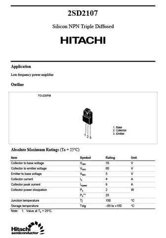
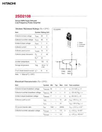
2SD2107 Silicon NPN Triple Diffused Application Low frequency power amplifier Outline TO-220FM 1. Base 2. Collector 3. Emitter 1 2 3 Absolute Maximum Ratings (Ta = 25 C) Item Symbol Rating Unit Collector to base voltage VCBO 70 V Collector to emitter voltage VCEO 60 V Emitter to base voltage VEBO 5V Collector current IC 4A Collector peak current IC(peak) 8A Collector power d
9.12. Size:35K hitachi
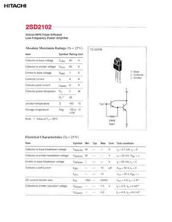
2sd2101.pdf

2SD2101 Silicon NPN Triple Diffused Application Low frequency power amplifier Outline TO-220FM 2 1 1. Base 2. Collector 3. Emitter 1 2 3 k 150 3 (Typ) (Typ) 3 2SD2101 Absolute Maximum Ratings (Ta = 25 C) Item Symbol Rating Unit Collector to base voltage VCBO 200 V Collector to emitter voltage VCEO 200 V Emitter to base voltage VEBO 7V Collector current IC 10 A Co
9.13. Size:29K calogic
sd210de sd212de sd214de.pdf
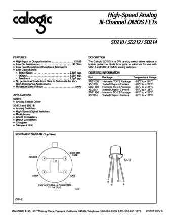
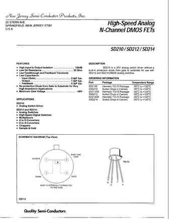
High-Speed Analog N-Channel DMOS FETs SD210 / SD212 / SD214 FEATURES DESCRIPTION High Input to Output Isolation . . . . . . . . . . . . . . . . 120dB The Calogic SD210 is a 30V analog switch driver without a Low On Resistance . . . . . . . . . . . . . . . . . . . . . . . . 30 Ohm built-in protection diode from gate to substrate for use with Low Feedthrough and Feedba
9.14. Size:103K jmnic
2sd2101.pdf
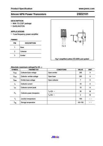
Product Specification www.jmnic.com Silicon NPN Power Transistors 2SD2101 DESCRIPTION With TO-220F package DARLINGTON APPLICATIONS Low frequency power amplifier PINNING PIN DESCRIPTION 1 Base 2 Collector 3 Emitter Fig.1 simplified outline (TO-220F) and symbol Absolute maximum ratings(Ta=25 ) SYMBOL PARAMETER CONDITIONS VALUE UNIT VCBO Collector-base voltage Op
9.15. Size:198K inchange semiconductor
2sd2104.pdf
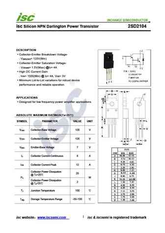
I isc Silicon NPN Darlington Power Transistor 2SD2104 DESCRIPTION Collector-Emitter Breakdown Voltage- V = 120V(Min) (BR)CEO Collector-Emitter Saturation Voltage- V = 1.5V(Max) @I = 4A CE(sat) C High DC Current Gain h = 1000(Min) @ I = 4A, V = 3V FE C CE Minimum Lot-to-Lot variations for robust device performance and reliable operation APPLICATIONS Designed for lo
9.16. Size:197K inchange semiconductor
2sd2105.pdf

isc Silicon NPN Darlington Power Transistor 2SD2105 DESCRIPTION Collector-Emitter Breakdown Voltage- V = 120V(Min) (BR)CEO Collector-Emitter Saturation Voltage- V = 1.5V(Max) @I = 5A CE(sat) C High DC Current Gain h = 1000(Min) @ I = 5A, V = 3V FE C CE Minimum Lot-to-Lot variations for robust device performance and reliable operation APPLICATIONS Designed for low f
9.17. Size:197K inchange semiconductor
2sd2106.pdf
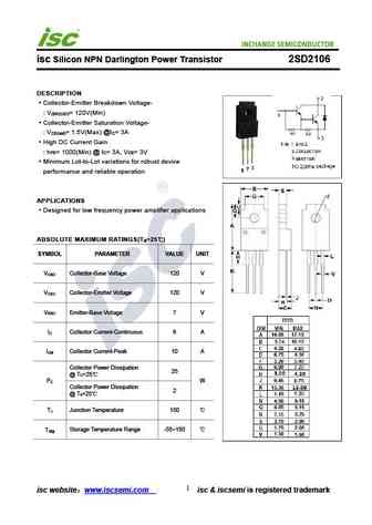
isc Silicon NPN Darlington Power Transistor 2SD2106 DESCRIPTION Collector-Emitter Breakdown Voltage- V = 120V(Min) (BR)CEO Collector-Emitter Saturation Voltage- V = 1.5V(Max) @I = 3A CE(sat) C High DC Current Gain h = 1000(Min) @ I = 3A, V = 3V FE C CE Minimum Lot-to-Lot variations for robust device performance and reliable operation APPLICATIONS Designed for low f
9.18. Size:198K inchange semiconductor
2sd2108.pdf

isc Silicon NPN Darlington Power Transistor 2SD2108 DESCRIPTION Collector-Emitter Breakdown Voltage- V = 80V(Min) (BR)CEO Collector-Emitter Saturation Voltage- V = 1.5V(Max) @I = 4A CE(sat) C High DC Current Gain h = 1000(Min) @ I = 4A, V = 3V FE C CE Minimum Lot-to-Lot variations for robust device performance and reliable operation APPLICATIONS Designed for low fr
9.19. Size:198K inchange semiconductor
2sd2107.pdf
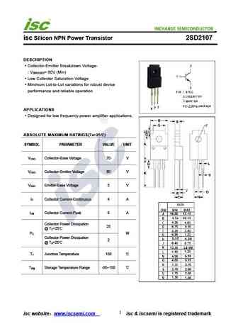
isc Silicon NPN Power Transistor 2SD2107 DESCRIPTION Collector-Emitter Breakdown Voltage- V = 60V (Min) (BR)CEO Low Collector Saturation Voltage Minimum Lot-to-Lot variations for robust device performance and reliable operation APPLICATIONS Designed for low frequency power amplifier applications. ABSOLUTE MAXIMUM RATINGS(T =25 ) a SYMBOL PARAMETER VALUE UNIT V Collector
9.20. Size:198K inchange semiconductor
2sd2101.pdf
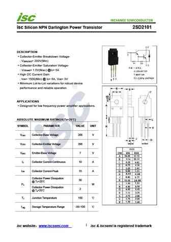
isc Silicon NPN Darlington Power Transistor 2SD2101 DESCRIPTION Collector-Emitter Breakdown Voltage- V = 200V(Min) (BR)CEO Collector-Emitter Saturation Voltage- V = 1.5V(Max) @I = 5A CE(sat) C High DC Current Gain h = 1500(Min) @ I = 5A, V = 3V FE C CE Minimum Lot-to-Lot variations for robust device performance and reliable operation APPLICATIONS Designed for low f
Otros transistores... IRF734PBF
, IRF7351PBF
, SD10425
, SD200DC
, SD201DC
, SD202DC
, SD203DC
, SD210
, 2N7002
, SD210DE
, SD212
, SD212DE
, SD214
, SD214DE
, SD217DE
, SD219DE
, SD403BD
.
History: 2SK3925-01
| SES759
| RU3070M3