IRFB59N10DPBF MOSFET Equivalente. Reemplazo. Hoja de especificaciones. Principales características
Número de Parte: IRFB59N10DPBF
Tipo de FET: MOSFET
Polaridad de transistor: N
ESPECIFICACIONES MÁXIMAS
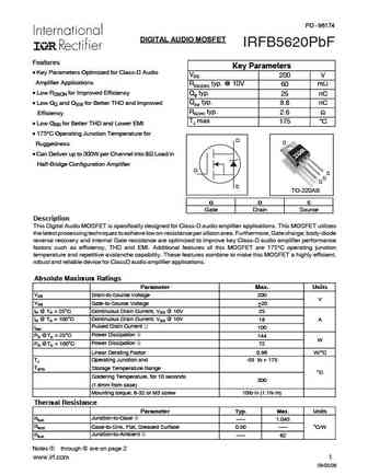
Pdⓘ - Máxima disipación de potencia: 200 W
|Vds|ⓘ - Voltaje máximo drenador-fuente: 100 V
|Vgs|ⓘ - Voltaje máximo fuente-puerta: 30 V
|Id|ⓘ - Corriente continua de drenaje: 59 A
Tjⓘ - Temperatura máxima de unión: 175 °C
CARACTERÍSTICAS ELÉCTRICAS
trⓘ - Tiempo de subida: 90 nS
Cossⓘ - Capacitancia de salida: 740 pF
RDSonⓘ - Resistencia estado encendido drenaje a fuente: 0.025 Ohm
Encapsulados: TO-220AB
Búsqueda de reemplazo de IRFB59N10DPBF MOSFET
- Selecciónⓘ de transistores por parámetros
IRFB59N10DPBF datasheet
irfb59n10dpbf irfs59n10dpbf.pdf
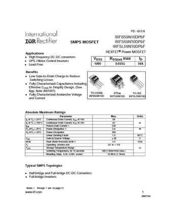
PD - 95378 IRFB59N10DPbF IRFS59N10DPbF SMPS MOSFET IRFSL59N10DPbF HEXFET Power MOSFET Applications l High frequency DC-DC converters VDSS RDS(on) max ID l UPS / Motor Control Inverters 100V 0.025 59A l Lead-Free Benefits l Low Gate-to-Drain Charge to Reduce Switching Losses l Fully Characterized Capacitance Including Effective COSS to Simplify Design, (See App. Note AN1
irfb59n10dpbf irfs59n10dpbf irfsl59n10dpbf.pdf

PD - 95378 IRFB59N10DPbF IRFS59N10DPbF SMPS MOSFET IRFSL59N10DPbF HEXFET Power MOSFET Applications l High frequency DC-DC converters VDSS RDS(on) max ID l UPS / Motor Control Inverters 100V 0.025 59A l Lead-Free Benefits l Low Gate-to-Drain Charge to Reduce Switching Losses l Fully Characterized Capacitance Including Effective COSS to Simplify Design, (See App. Note AN1
irfb59n10d.pdf
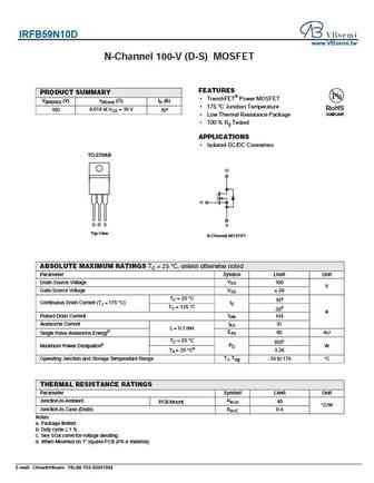
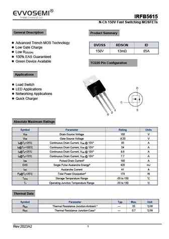
IRFB59N10D www.VBsemi.tw N-Channel 100-V (D-S) MOSFET FEATURES PRODUCT SUMMARY TrenchFET Power MOSFET V(BR)DSS (V) rDS(on) ( )ID (A) 175 C Junction Temperature RoHS 0.018 at VGS = 10 V 100 70a COMPLIANT Low Thermal Resistance Package 100 % Rg Tested APPLICATIONS Isolated DC/DC Converters TO-220AB D G G D S S Top View N-Channel MOSFET ABSOLUTE
irfb59n10d.pdf
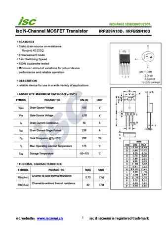
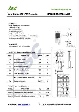
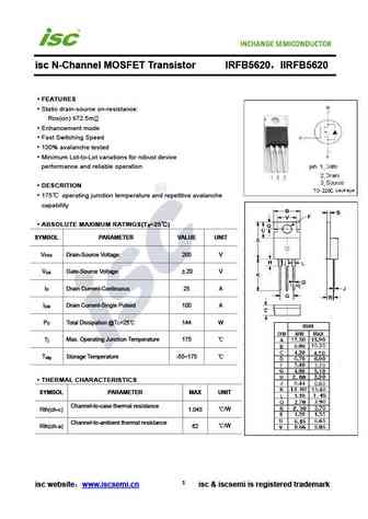
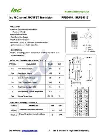
INCHANGE Semiconductor isc N-Channel MOSFET Transistor IRFB59N10D IIRFB59N10D FEATURES Static drain-source on-resistance RDS(on) 0.025 Enhancement mode Fast Switching Speed 100% avalanche tested Minimum Lot-to-Lot variations for robust device performance and reliable operation DESCRITION reliable device for use in a wide variety of applications ABSOLUTE MA
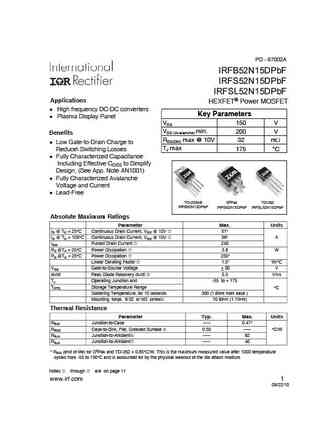


Otros transistores... IRFB4510PBF , IRFB4610PBF , IRFB4615PBF , IRFB4620PBF , IRFB4710PBF , IRFB52N15DPBF , IRFB5615PBF , IRFB5620PBF , IRFB31N20D , IRFB61N15DPBF , IRFB9N30APBF , IRFB9N60APBF , IRFB9N65APBF , IRFBA1404PPBF , IRFBA1405PPBF , IRFBA22N50APBF , IRFBA90N20DPBF .
🌐 : EN ES РУ

Liste
Recientemente añadidas las descripciónes de los transistores:
MOSFET: AUB034N10 | AUB033N08BG | AUB026N085 | AUA062N08BG | AUA060N08AG | AUA056N08BGL | AUA039N10 | ASW80R290E | ASW65R120EFD | ASW65R110E | ASW65R095EFD | ASW65R046EFD | ASW65R041EFDA | ASW65R041E | ASW60R150E | ASW60R090EFDA
Popular searches
bc183l | tip35 datasheet | tip36c datasheet | 2sc461 | hy1906 | 2sc2238 | 2sc458 transistor | b649a transistor