2SJ460 MOSFET Equivalente. Reemplazo. Hoja de especificaciones. Principales características
Número de Parte: 2SJ460
Tipo de FET: MOSFET
Polaridad de transistor: P
ESPECIFICACIONES MÁXIMAS
Pdⓘ - Máxima disipación de potencia: 0.25
W
|Vds|ⓘ - Voltaje máximo drenador - fuente: 50
V
|Vgs|ⓘ - Voltaje máximo fuente - puerta: 7
V
|Id|ⓘ - Corriente continua de drenaje: 0.1
A
Tjⓘ - Temperatura máxima de unión: 150
°C
CARACTERÍSTICAS ELÉCTRICAS
trⓘ - Tiempo de subida: 270
nS
Cossⓘ - Capacitancia
de salida: 9
pF
Rds(on)ⓘ - Resistencia estado encendido drenaje a fuente: 50
Ohm
Paquete / Cubierta:
SST
Búsqueda de reemplazo de 2SJ460 MOSFET
-
Selección ⓘ de transistores por parámetros
Principales características: 2SJ460
9.3. Size:371K toshiba
2sj465.pdf 
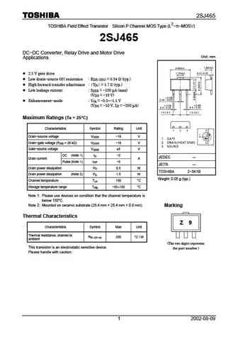
2SJ465 2 TOSHIBA Field Effect Transistor Silicon P Channel MOS Type (L - -MOSV) 2SJ465 DC-DC Converter, Relay Drive and Motor Drive Unit mm Applications 2.5 V gate drive Low drain-source ON resistance R = 0.54 (typ.) DS (ON) High forward transfer admittance Y = 1.7 S (typ.) fs Low leakage current I = -100 A (max) DSS (V = -16 V) DS Enhance
9.4. Size:39K sanyo
2sj466.pdf 
Ordering number ENN5491B P-Channel Silicon MOSFET 2SJ466 Ultrahigh-Speed Switching Applications Features Package Dimensions Low ON resistance. unit mm Ultrahigh-speed switching. 2128 4V drive. [2SJ466] Enables simplified fabrication, high-density mount- 8.2 7.8 ing, and miniaturization in end products due to the 6.2 0.6 3 surface mountable package. 1 2 0.3 1
9.5. Size:246K renesas
2sj463a.pdf 
To our customers, Old Company Name in Catalogs and Other Documents On April 1st, 2010, NEC Electronics Corporation merged with Renesas Technology Corporation, and Renesas Electronics Corporation took over all the business of both companies. Therefore, although the old company name remains in this document, it is a valid Renesas Electronics document. We appreciate your understanding.
9.6. Size:62K nec
2sj462.pdf 
DATA SHEET MOS FIELD EFFECT TRANSISTOR 2SJ462 P-CHANNEL MOS FIELD EFFECT TRANSISTOR FOR HIGH SPEED SWITCHING DESCRIPTION Package Drawings (unit mm) The 2SJ462 is a switching device which can be driven directly 5.7 0.1 by an IC operating at 3 V. 1.5 0.1 2.0 0.2 The 2SJ462 features a low on-state resistance and can be driven by a low voltage power source, so it is suitable for
9.7. Size:723K nec
2sj461a.pdf 
DATA SHEET MOS FIELD EFFECT TRANSISTOR 2SJ461A P-CHANNEL MOSFET FOR HIGH SPEED SWITCHING DESCRIPTION The 2SJ461A is a switching device which can be driven directly by a 2.5 V power source. The 2SJ461A has excellent switching characteristics and is suitable for use as a high-speed switching device in digital circuit. FEATURES PACKAGE DRAWING (Unit mm) Can be driven by a
9.8. Size:138K nec
2sj463a.pdf 
DATA SHEET MOS FIELD EFFECT TRANSISTOR 2SJ463A P-CHANNEL MOS FIELD EFFECT TRANSISTOR FOR HIGH SPEED SWITCHING PACKAGE DRAWING (Unit mm) DESCRIPTION The 2SJ463A is a switching device which can be driven directly 2.1 0.1 by a 2.5 V power source. 1.25 0.1 The 2SJ463A has excellent switching characteristics, and is suitable for use as a high-speed switching device in digita
9.9. Size:711K nec
2sj461.pdf 
DATA SHEET MOS FIELD EFFECT TRANSISTOR 2SJ461 P-CHANNEL MOS FIELD EFFECT TRANSISTOR FOR HIGH SPEED SWITCHING PACKAGE DRAWING (Unit mm) DESCRIPTION The 2SJ461 is a switching device which can be driven directly 2.8 0.2 by a 2.5 V power source. +0.1 0.65 0.15 1.5 The 2SJ461 has excellent switching characteristics and is suitable for use as a high-speed switching device
9.10. Size:1139K kexin
2sj461-3.pdf 
SMD Type MOSFET P-Channel MOSFET 2SJ461 SOT-23-3 Unit mm +0.2 2.9 -0.1 +0.1 0.4-0.1 3 Features VDS (V) =-50V 1 2 ID =-0.1 A +0.02 +0.1 0.15 -0.02 0.95 -0.1 +0.1 RDS(ON) 50 (VGS =-4V) 1.9 -0.2 RDS(ON) 100 (VGS =-2.5V) 1. Gate 2. Source 3. Drain Absolute Maximum Ratings Ta = 25 Parameter Symbol Rating Unit Drain-Source Voltag
9.11. Size:1130K kexin
2sj461.pdf 
SMD Type MOSFET P-Channel MOSFET 2SJ461 SOT-23 Unit mm +0.1 2.9-0.1 +0.1 0.4 -0.1 3 Features VDS (V) =-50V 1 2 ID =-0.1 A +0.1 +0.05 0.95 -0.1 0.1 -0.01 RDS(ON) 50 (VGS =-4V) 1.9+0.1 -0.1 RDS(ON) 100 (VGS =-2.5V) 1. Gate 2. Source 3. Drain Absolute Maximum Ratings Ta = 25 Parameter Symbol Rating Unit Drain-Source Voltage VDS
Otros transistores... 2SJ353
, 2SJ411
, 2SJ424
, 2SJ425
, 2SJ44
, 2SJ448
, 2SJ449
, 2SJ45
, 5N60
, 2SJ461
, 2SJ462
, 2SJ463
, 2SJ471
, 2SJ479
, 2SJ483
, 2SJ484
, 2SJ486
.