HFD5N70S MOSFET Equivalente. Reemplazo. Hoja de especificaciones. Principales características
Número de Parte: HFD5N70S
Tipo de FET: MOSFET
Polaridad de transistor: N
ESPECIFICACIONES MÁXIMAS
Pdⓘ - Máxima
disipación de potencia: 91 W
|Vds|ⓘ - Voltaje máximo drenador-fuente: 700 V
|Vgs|ⓘ - Voltaje máximo fuente-puerta: 30 V
|Id|ⓘ - Corriente continua
de drenaje: 3.8 A
Tjⓘ - Temperatura máxima de unión: 150 °C
CARACTERÍSTICAS ELÉCTRICAS
trⓘ - Tiempo
de subida: 45 nS
Cossⓘ - Capacitancia de salida: 60 pF
RDSonⓘ - Resistencia estado encendido drenaje a fuente: 3.2 Ohm
Encapsulados: D-PAK
Búsqueda de reemplazo de HFD5N70S MOSFET
- Selecciónⓘ de transistores por parámetros
HFD5N70S datasheet
..1. Size:169K semihow
hfd5n70s.pdf 

Jan 2013 BVDSS = 700 V RDS(on) typ HFD5N70S / HFU5N70S ID = 3.8 A 700V N-Channel MOSFET D-PAK I-PAK 2 FEATURES 1 1 3 2 3 Originative New Design HFD5N70S HFU5N70S Superior Avalanche Rugged Technology 1.Gate 2. Drain 3. Source Robust Gate Oxide Technology Very Low Intrinsic Capacitances Excellent Switching Characteristics Unrivalled Gate Charge 10.5 nC
7.1. Size:209K semihow
hfd5n70u.pdf

Jan 2014 BVDSS = 700 V RDS(on) typ = 2.7 HFD5N70U / HFU5N70U ID = 3.6 A 700V N-Channel MOSFET D-PAK I-PAK FEATURES 2 1 Originative New Design 1 3 2 3 Superior Avalanche Rugged Technology HFD5N70U HFU5N70U Robust Gate Oxide Technology 1.Gate 2. Drain 3. Source Very Low Intrinsic Capacitances Excellent Switching Characteristics Unrivalled Gate Charge 10.5 nC
9.1. Size:199K semihow
hfd5n40.pdf

July 2005 BVDSS = 400 V RDS(on) typ HFD5N40 / HFU5N40 ID = 3.4 A 400V N-Channel MOSFET D-PAK I-PAK 2 FEATURES 1 1 3 2 3 Originative New Design HFD5N40 HFU5N40 Superior Avalanche Rugged Technology 1.Gate 2. Drain 3. Source Robust Gate Oxide Technology Very Low Intrinsic Capacitances Excellent Switching Characteristics Unrivalled Gate Charge 13 nC (Typ
9.2. Size:205K semihow
hfd5n60s.pdf

Sep 2009 BVDSS = 600 V RDS(on) typ = 2.0 HFD5N60S / HFU5N60S ID = 4.3 A 600V N-Channel MOSFET D-PAK I-PAK 2 2 FEATURES 1 1 3 2 3 Originative New Design HFD5N60S HFU5N60S Superior Avalanche Rugged Technology 1.Gate 2. Drain 3. Source Robust Gate Oxide Technology Very Low Intrinsic Capacitances Excellent Switching Characteristics Unrivalled Gate Charge 10.5 nC (Typ
9.3. Size:324K semihow
hfd5n60s hfu5n60s.pdf
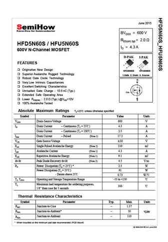
June 2015 BVDSS = 600 V RDS(on) typ HFD5N60S / HFU5N60S ID = 4.3 A 600V N-Channel MOSFET D-PAK I-PAK 2 FEATURES 1 1 3 2 3 Originative New Design HFD5N60S HFU5N60S Superior Avalanche Rugged Technology 1.Gate 2. Drain 3. Source Robust Gate Oxide Technology Very Low Intrinsic Capacitances Excellent Switching Characteristics Unrivalled Gate Charge 10.5 nC
9.4. Size:276K semihow
hfd5n50s.pdf
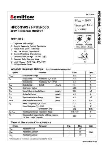
OCT 2009 BVDSS = 500 V RDS(on) typ HFD5N50S / HFU5N50S ID = 4.0 A 500V N-Channel MOSFET D-PAK I-PAK 2 FEATURES 1 1 3 2 3 Originative New Design HFD5N50S HFU5N50S Superior Avalanche Rugged Technology 1.Gate 2. Drain 3. Source Robust Gate Oxide Technology Very Low Intrinsic Capacitances Excellent Switching Characteristics Unrivalled Gate Charge 15.5 nC
9.5. Size:209K semihow
hfd5n65u.pdf

Jan 2014 BVDSS = 650 V RDS(on) typ = 2.3 HFD5N65U / HFU5N65U ID = 3.6 A 650V N-Channel MOSFET D-PAK I-PAK FEATURES 2 1 Originative New Design 1 3 2 3 Superior Avalanche Rugged Technology HFD5N65U HFU5N65U Robust Gate Oxide Technology 1.Gate 2. Drain 3. Source Very Low Intrinsic Capacitances Excellent Switching Characteristics Unrivalled Gate Charge 10.5 nC
9.6. Size:276K semihow
hfd5n50s hfu5n50s.pdf

OCT 2009 BVDSS = 500 V RDS(on) typ HFD5N50S / HFU5N50S ID = 4.0 A 500V N-Channel MOSFET D-PAK I-PAK 2 FEATURES 1 1 3 2 3 Originative New Design HFD5N50S HFU5N50S Superior Avalanche Rugged Technology 1.Gate 2. Drain 3. Source Robust Gate Oxide Technology Very Low Intrinsic Capacitances Excellent Switching Characteristics Unrivalled Gate Charge 15.5 nC
9.7. Size:210K semihow
hfd5n60u.pdf
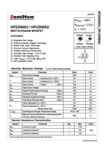
Jan 2014 BVDSS = 600 V RDS(on) typ = 2.0 HFD5N60U / HFU5N60U ID = 3.6 A 600V N-Channel MOSFET D-PAK I-PAK FEATURES 2 1 Originative New Design 1 3 2 3 Superior Avalanche Rugged Technology HFD5N60U HFU5N60U Robust Gate Oxide Technology 1.Gate 2. Drain 3. Source Very Low Intrinsic Capacitances Excellent Switching Characteristics Unrivalled Gate Charge 10.5 nC
9.8. Size:207K semihow
hfd5n50u.pdf

Jan 2014 BVDSS = 500 V RDS(on) typ HFD5N50U / HFU5N50U ID = 4.0 A 500V N-Channel MOSFET D-PAK I-PAK FEATURES 2 1 Originative New Design 1 3 2 3 Superior Avalanche Rugged Technology HFD5N50U HFU5N50U Robust Gate Oxide Technology 1.Gate 2. Drain 3. Source Very Low Intrinsic Capacitances Excellent Switching Characteristics Unrivalled Gate Charge 13 nC (
9.9. Size:357K semihow
hfd5n60u hfu5n60u.pdf

June 2015 BVDSS = 600 V RDS(on) typ = 2.0 HFD5N60U / HFU5N60U ID = 3.6 A 600V N-Channel MOSFET D-PAK I-PAK FEATURES 2 1 Originative New Design 1 3 2 3 Superior Avalanche Rugged Technology HFD5N60U HFU5N60U Robust Gate Oxide Technology 1.Gate 2. Drain 3. Source Very Low Intrinsic Capacitances Excellent Switching Characteristics Unrivalled Gate Charge 10.5 nC
9.10. Size:199K semihow
hfd5n40 hfu5n40.pdf
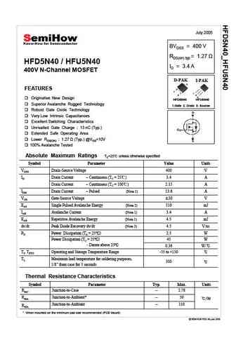
July 2005 BVDSS = 400 V RDS(on) typ HFD5N40 / HFU5N40 ID = 3.4 A 400V N-Channel MOSFET D-PAK I-PAK 2 FEATURES 1 1 3 2 3 Originative New Design HFD5N40 HFU5N40 Superior Avalanche Rugged Technology 1.Gate 2. Drain 3. Source Robust Gate Oxide Technology Very Low Intrinsic Capacitances Excellent Switching Characteristics Unrivalled Gate Charge 13 nC (Typ
9.11. Size:287K semihow
hfd5n50u hfu5n50u.pdf

June 2015 BVDSS = 500 V RDS(on) typ HFD5N50U / HFU5N50U ID = 4.0 A 500V N-Channel MOSFET D-PAK I-PAK FEATURES 2 1 Originative New Design 1 3 2 3 Superior Avalanche Rugged Technology HFD5N50U HFU5N50U Robust Gate Oxide Technology 1.Gate 2. Drain 3. Source Very Low Intrinsic Capacitances Excellent Switching Characteristics Unrivalled Gate Charge 13 nC
9.12. Size:1121K semihow
hfu5n65sa hfd5n65sa.pdf
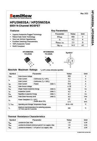
May. 2022 HFU5N65SA / HFD5N65SA 650V N-Channel MOSFET Features Key Parameters Parameter Value Unit Superior Avalanche Rugged Technology BVDSS 650 V Robust Gate Oxide Technology Very Low Intrinsic Capacitances ID 4.2 A Excellent Switching Characteristics RDS(on), Typ 2.3 100% Avalanche Tested Qg, Typ 14.2 nC RoHS Compliant HFU5N65SA HFD5N65SA Symbol TO
9.13. Size:291K semihow
hfu5n60f hfd5n60f.pdf
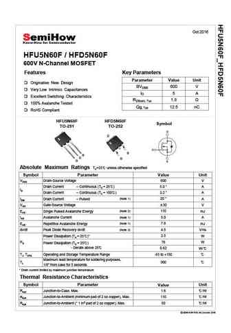
Oct 2016 HFU5N60F / HFD5N60F 600V N-Channel MOSFET Features Key Parameters Parameter Value Unit Originative New Design BVDSS 600 V Very Low Intrinsic Capacitances ID 5A Excellent Switching Characteristics RDS(on), Typ 1.8 100% Avalanche Tested Qg, Typ 12.5 nC RoHS Compliant HFU5N60F HFD5N60F Symbol TO-251 TO-252 D S S D G G Absolute Maximum Ratings TC=25 unles
9.14. Size:204K semihow
hfd5n65s.pdf
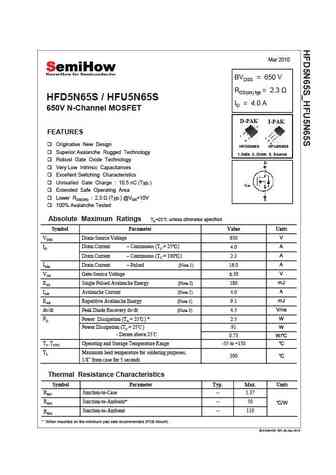
Mar 2010 BVDSS = 650 V RDS(on) typ = 2.3 HFD5N65S / HFU5N65S ID = 4.0 A 650V N-Channel MOSFET D-PAK I-PAK 2 2 FEATURES 1 1 3 2 3 Originative New Design HFD5N65S HFU5N65S Superior Avalanche Rugged Technology 1.Gate 2. Drain 3. Source Robust Gate Oxide Technology Very Low Intrinsic Capacitances Excellent Switching Characteristics Unrivalled Gate Charge 10.5 nC (Typ
Otros transistores... HFD4N50
, HFD5N40
, HFD5N50S
, HFD5N50U
, HFD5N60S
, HFD5N60U
, HFD5N65S
, HFD5N65U
, IRF1405
, HFD5N70U
, HFD630
, HFD6N60U
, HFD6N65U
, HFD6N70U
, HFD8N60U
, HFD8N65U
, HFD8N70U
.
