NDS355AN Datasheet. Equivalente. Reemplazo. Hoja de especificaciones. Principales características
Número de Parte: NDS355AN 📄📄
Tipo de FET: MOSFET
Polaridad de transistor: N
ESPECIFICACIONES MÁXIMAS
Pdⓘ - Máxima disipación de potencia: 0.5 W
|Vds|ⓘ - Voltaje máximo drenador-fuente: 30 V
|Vgs|ⓘ - Voltaje máximo fuente-puerta: 20 V
|Id|ⓘ - Corriente continua de drenaje: 1.7 A
Tjⓘ - Temperatura máxima de unión: 150 °C
CARACTERÍSTICAS ELÉCTRICAS
RDSonⓘ - Resistencia estado encendido drenaje a fuente: 0.085 Ohm
Encapsulados: SUPERSOT3
📄📄 Copiar
Búsqueda de reemplazo de NDS355AN MOSFET
- Selecciónⓘ de transistores por parámetros
NDS355AN datasheet
..1. Size:65K fairchild semi
nds355an.pdf 
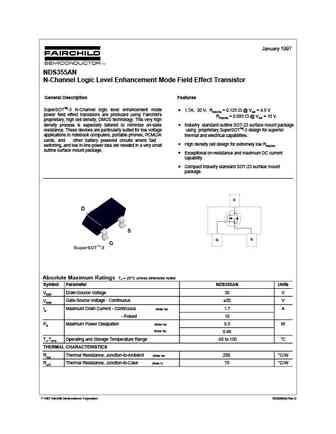
January 1997 NDS355AN N-Channel Logic Level Enhancement Mode Field Effect Transistor General Description Features SuperSOTTM-3 N-Channel logic level enhancement mode 1.7A, 30 V, RDS(ON) = 0.125 @ VGS = 4.5 V power field effect transistors are produced using Fairchild's RDS(ON) = 0.085 @ VGS = 10 V. proprietary, high cell density, DMOS technology. This very high density proce
..2. Size:464K onsemi
nds355an.pdf
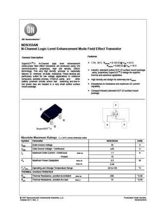
NDS355AN N-Channel Logic Level Enhancement Mode Field Effect Transistor Features General Description 1.7A, 30 V, RDS(ON) = 0.125 @ VGS = 4.5 V SuperSOTTM-3 N-Channel logic level enhancement RDS(ON) = 0.085 @ VGS = 10 V. mode power field effect transistors are produced using ON Semiconductor's proprietary, high cell density, DMOS Industry standard outline SOT-23 surface mou
8.1. Size:58K fairchild semi
nds355n.pdf
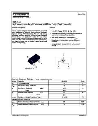
March 1996 NDS355N N-Channel Logic Level Enhancement Mode Field Effect Transistor General Description Features These N-Channel logic level enhancement mode power field 1.6A, 30V. RDS(ON) = 0.125 @ VGS = 4.5V. effect transistors are produced using Fairchild's proprietary, Proprietary package design using copper lead frame for high cell density, DMOS technology. This very high densi
8.2. Size:177K onsemi
nds355n.pdf

Is Now Part of To learn more about ON Semiconductor, please visit our website at www.onsemi.com Please note As part of the Fairchild Semiconductor integration, some of the Fairchild orderable part numbers will need to change in order to meet ON Semiconductor s system requirements. Since the ON Semiconductor product management systems do not have the ability to manage part nomenclatur
9.1. Size:80K fairchild semi
nds351n.pdf
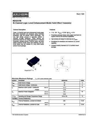
March 1996 NDS351N N-Channel Logic Level Enhancement Mode Field Effect Transistor General Description Features These N-Channel logic level enhancement mode power 1.1A, 30V. RDS(ON) = 0.25 @ VGS = 4.5V. field effect transistors are produced using Fairchild's Proprietary package design using copper lead frame for proprietary, high cell density, DMOS technology. This superior thermal
9.2. Size:127K fairchild semi
nds351an.pdf
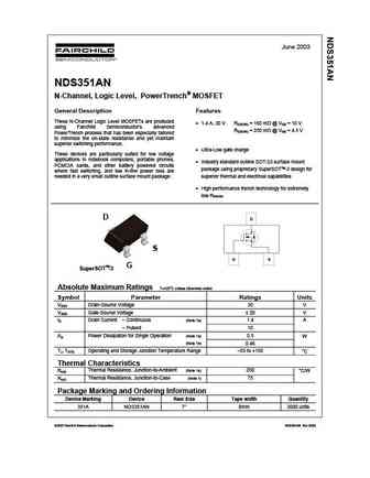
June 2003 NDS351AN N-Channel, Logic Level, PowerTrench MOSFET General Description Features These N-Channel Logic Level MOSFETs are produced 1.4 A, 30 V. RDS(ON) = 160 m @ VGS = 10 V using Fairchild Semiconductor s advanced RDS(ON) = 250 m @ VGS = 4.5 V PowerTrench process that has been especially tailored to minimize the on-state resistance and yet maintain superior switc
9.3. Size:84K fairchild semi
nds356p.pdf
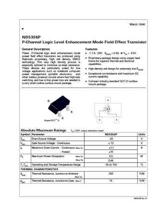
March 1996 N NDS356P P-Channel Logic Level Enhancement Mode Field Effect Transistor General Description Features These P-Channel logic level enhancement mode -1.1 A, -20V. RDS(ON) = 0.3 @ VGS = -4.5V. power field effect transistors are produced using Proprietary package design using copper lead Nationals proprietary, high cell density, DMOS frame for superior thermal and electrical
9.4. Size:62K fairchild semi
nds352p.pdf
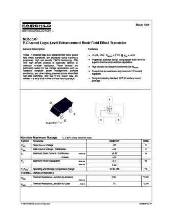
March 1996 NDS352P P-Channel Logic Level Enhancement Mode Field Effect Transistor General Description Features These P-Channel logic level enhancement mode power -0.85A, -20V. RDS(ON) = 0.5 @ VGS = -4.5V. field effect transistors are produced using Fairchild's Proprietary package design using copper lead frame for proprietary, high cell density, DMOS technology. This superior therma
9.5. Size:154K onsemi
nds356ap.pdf
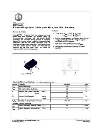
NDS356AP P-Channel Logic Level Enhancement Mode Field Effect Transistor Features General Description -1.1 A, -30 V, RDS(ON) = 0.3 @ VGS=-4.5 V SuperSOTTM-3 P-Channel logic level enhancement mode RDS(ON) = 0.2 @ VGS=-10 V. power field effect transistors are produced using ON Semiconductor's proprietary, high cell density, DMOS Industry standard outline SOT-23 surface mount
9.6. Size:202K onsemi
nds352ap.pdf

Is Now Part of To learn more about ON Semiconductor, please visit our website at www.onsemi.com Please note As part of the Fairchild Semiconductor integration, some of the Fairchild orderable part numbers will need to change in order to meet ON Semiconductor s system requirements. Since the ON Semiconductor product management systems do not have the ability to manage part nomenclatur
9.7. Size:197K onsemi
nds351n.pdf

Is Now Part of To learn more about ON Semiconductor, please visit our website at www.onsemi.com Please note As part of the Fairchild Semiconductor integration, some of the Fairchild orderable part numbers will need to change in order to meet ON Semiconductor s system requirements. Since the ON Semiconductor product management systems do not have the ability to manage part nomenclatur
9.8. Size:244K onsemi
nds351an.pdf

Is Now Part of To learn more about ON Semiconductor, please visit our website at www.onsemi.com Please note As part of the Fairchild Semiconductor integration, some of the Fairchild orderable part numbers will need to change in order to meet ON Semiconductor s system requirements. Since the ON Semiconductor product management systems do not have the ability to manage part nomenclatur
9.9. Size:1668K kexin
nds352ap.pdf
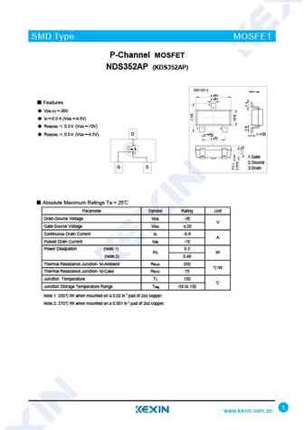
SMD Type MOSFET P-Channel MOSFET NDS352AP (KDS352AP) SOT-23-3 Unit mm +0.2 2.9-0.1 +0.1 0.4 -0.1 Features 3 VDS (V) =-30V ID =-0.9 A (VGS =-4.5V) RDS(ON) 0.3 (VGS =-10V) 1 2 +0.02 +0.1 0.15 -0.02 D 0.95 -0.1 RDS(ON) 0.5 (VGS =-4.5V) 1.9+0.1 -0.2 1.Gate 2.Source G S 3.Drain Absolute Maximum Ratings Ta = 25 Parameter Symbol Ra
9.10. Size:1477K cn vbsemi
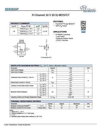
nds356ap.pdf

NDS356AP www.VBsemi.tw P-Channel 30 V (D-S) MOSFET FEATURES PRODUCT SUMMARY TrenchFET Power MOSFET 100 % Rg Tested VDS (V) RDS(on) ( ) Typ. ID (A)a Qg (Typ.) 0.046 at VGS = - 10 V - 5.6 0.049 at VGS = - 6 V - 5 11.4 nC - 30 APPLICATIONS 0.054 at VGS = - 4.5 V -4.5 For Mobile Computing - Load Switch - Notebook Adaptor Switch S TO-236 - DC/DC Converter (SOT-23
9.11. Size:849K cn vbsemi
nds352ap.pdf
NDS352AP www.VBsemi.tw P-Channel 30 V (D-S) MOSFET FEATURES PRODUCT SUMMARY TrenchFET Power MOSFET 100 % Rg Tested VDS (V) RDS(on) ( ) Typ. ID (A)a Qg (Typ.) 0.046 at VGS = - 10 V - 5.6 0.049 at VGS = - 6 V - 5 11.4 nC - 30 APPLICATIONS 0.054 at VGS = - 4.5 V -4.5 For Mobile Computing - Load Switch - Notebook Adaptor Switch S TO-236 - DC/DC Converter (SOT-23
Otros transistores... NDP7061L, NDP708A, NDP710A, NDS0605, NDS0610, NDS332P, NDS351AN, NDS352AP, K3569, NDS356AP, NDS7002A, NDS8410A, NDS8425, NDS8426A, NDS8434A, NDS8435A, NDS8926
