NDS8410A Datasheet. Equivalente. Reemplazo. Hoja de especificaciones. Principales características
Número de Parte: NDS8410A 📄📄
Tipo de FET: MOSFET
Polaridad de transistor: N
ESPECIFICACIONES MÁXIMAS
Pdⓘ - Máxima disipación de potencia: 2.5 W
|Vds|ⓘ - Voltaje máximo drenador-fuente: 30 V
|Vgs|ⓘ - Voltaje máximo fuente-puerta: 20 V
|Id|ⓘ - Corriente continua de drenaje: 10.8 A
Tjⓘ - Temperatura máxima de unión: 150 °C
CARACTERÍSTICAS ELÉCTRICAS
RDSonⓘ - Resistencia estado encendido drenaje a fuente: 0.012 Ohm
Encapsulados: SO8
📄📄 Copiar
Búsqueda de reemplazo de NDS8410A MOSFET
- Selecciónⓘ de transistores por parámetros
NDS8410A datasheet
nds8410a.pdf
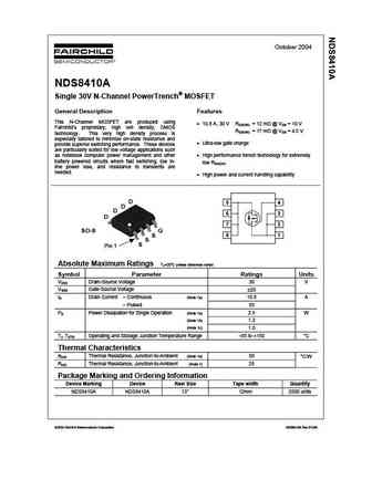
October 2004 NDS8410A Single 30V N-Channel PowerTrench MOSFET General Description Features This N-Channel MOSFET are produced using 10.8 A, 30 V RDS(ON) = 12 m @ VGS = 10 V Fairchild s proprietary, high cell density, DMOS RDS(ON) = 17 m @ VGS = 4.5 V technology. This very high density process is especially tailored to minimize on-state resistance and Ultra-low gate ch
nds8410.pdf
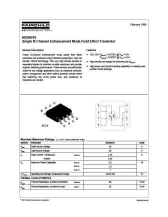
February 1996 NDS8410 Single N-Channel Enhancement Mode Field Effect Transistor General Description Features 10A, 30V. RDS(ON) = 0.015 @ VGS = 10V These N-Channel enhancement mode power field effect RDS(ON) = 0.020 @ VGS = 4.5V. transistors are produced using Fairchild's proprietary, high cell density, DMOS technology. This very high density process is High density cell design
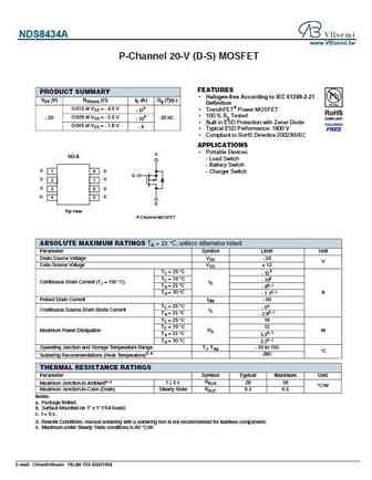
nds8434.pdf
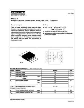
June 1996 NDS8434 Single P-Channel Enhancement Mode Field Effect Transistor General Description Features These P-Channel enhancement mode power field effect -6.5A, -20V. RDS(ON) = 0.035 @ VGS = -4.5V transistors are produced using Fairchild's proprietary, high cell RDS(ON) = 0.05 @ VGS = -2.7V. density, DMOS technology. This very high density process is High density cell design fo
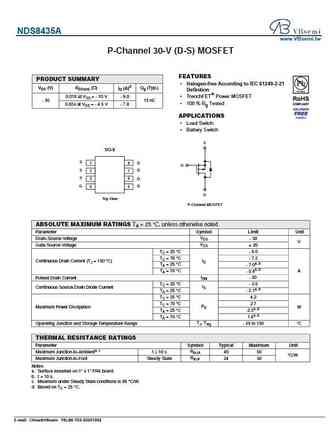
nds8435a.pdf
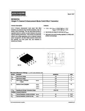
March 1997 NDS8435A Single P-Channel Enhancement Mode Field Effect Transistor General Description Features SO-8 P-Channel enhancement mode power field effect -7.9 A, -30 V. RDS(ON) = 0.023 @ VGS = -10 V transistors are produced using Fairchild's proprietary, high cell RDS(ON) = 0.035 @ VGS = -4.5V. density, DMOS technology. This very high density process is High density cell
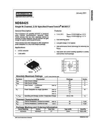

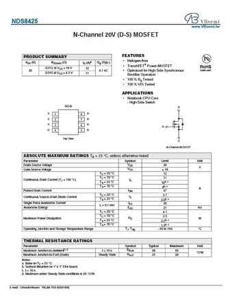
Otros transistores... NDS0605, NDS0610, NDS332P, NDS351AN, NDS352AP, NDS355AN, NDS356AP, NDS7002A, IRF530, NDS8425, NDS8426A, NDS8434A, NDS8435A, NDS8926, NDS8934, NDS8936, NDS8961
Parámetros del MOSFET. Cómo se afectan entre sí.
🌐 : EN ES РУ

Liste
Recientemente añadidas las descripciónes de los transistores:
MOSFET: MSQ60P04D | MSQ40P07D | MSQ30P40D | MSQ30P15 | MSQ30P07D | MSQ100N03D | MSHM60P14 | MSHM40N085 | MSHM30N46 | MSH60N35D | MSH40N032 | MSH30P100 | MSH100N045SA | MSD60P16 | MSD40P45 | MSB100N023
Popular searches
mp1620 | kta1381 | bf494 | 2sc1885 | skd502t | 2sb754 | 2sc2362 | 2sd468