APT5017SVFRG MOSFET Equivalente. Reemplazo. Hoja de especificaciones. Principales características
Número de Parte: APT5017SVFRG
Tipo de FET: MOFETS
Polaridad de transistor: N
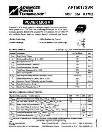
ESPECIFICACIONES MÁXIMAS
Pdⓘ - Máxima disipación de potencia: 370 W
|Vds|ⓘ - Voltaje máximo drenador-fuente: 500 V
|Vgs|ⓘ - Voltaje máximo fuente-puerta: 30 V
|Id|ⓘ - Corriente continua de drenaje: 30 A
Tjⓘ - Temperatura máxima de unión: 150 °C
CARACTERÍSTICAS ELÉCTRICAS
trⓘ - Tiempo de subida: 14 nS
Cossⓘ - Capacitancia de salida: 600 pF
RDSonⓘ - Resistencia estado encendido drenaje a fuente: 0.17 Ohm
Encapsulados: D3PAK
Búsqueda de reemplazo de APT5017SVFRG MOSFET
- Selecciónⓘ de transistores por parámetros
APT5017SVFRG datasheet
apt5017svfrg.pdf
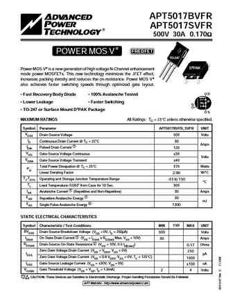
APT5017BVFR APT5017SVFR 500V 30A 0.170 POWER MOS V FREDFET TO-247 D3PAK Power MOS V is a new generation of high voltage N-Channel enhancement mode power MOSFETs. This new technology minimizes the JFET effect, increases packing density and reduces the on-resistance. Power MOS V also achieves faster switching speeds through optimized gate layout. D Fast
apt5017svr.pdf

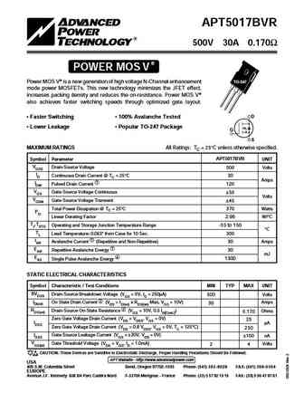
APT5017SVR 500V 30A 0.170 POWER MOS V Power MOS V is a new generation of high voltage N-Channel enhancement D3PAK mode power MOSFETs. This new technology minimizes the JFET effect, increases packing density and reduces the on-resistance. Power MOS V also achieves faster switching speeds through optimized gate layout. D Faster Switching 100% Avalanche Tested Lower L
apt5017blc.pdf
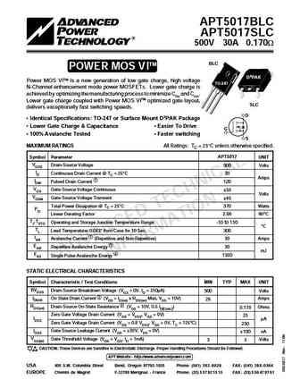
APT5017BLC APT5017SLC 500V 30A 0.170W BLC TM POWER MOS VI D3PAK Power MOS VITM is a new generation of low gate charge, high voltage TO-247 N-Channel enhancement mode power MOSFETs. Lower gate charge is achieved by optimizing the manufacturing process to minimize Ciss and Crss. Lower gate charge coupled with Power MOS VITM optimized gate layout, SLC delivers exceptionally fast switc
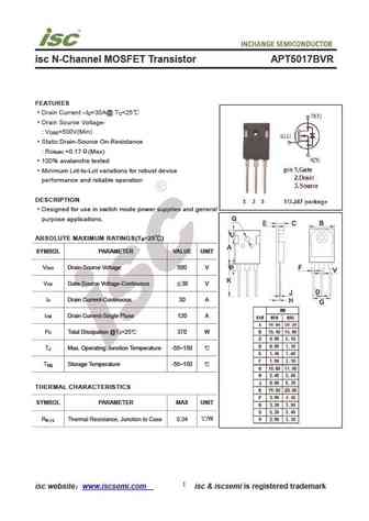
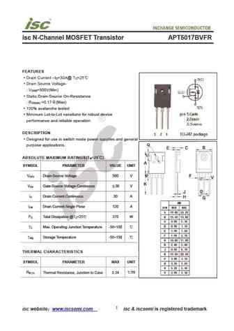
apt5017bvr.pdf
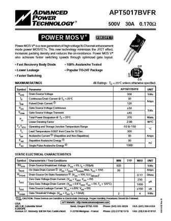
APT5017BVR 500V 30A 0.170 POWER MOS V Power MOS V is a new generation of high voltage N-Channel enhancement TO-247 mode power MOSFETs. This new technology minimizes the JFET effect, increases packing density and reduces the on-resistance. Power MOS V also achieves faster switching speeds through optimized gate layout. D Faster Switching 100% Avalanche Tested Lower
Otros transistores... BUK457-400B , 2SK125 , 2SJ410 , 2SK2518-01MR , 2SK4027 , APT5016BFLLG , APT5016BLLG , APT5016SFLLG , IRF1405 , APT5018BFLLG , APT5018SFLLG , APT5018SLL , APT5022BN , APT5024BLL , APT5024BLLG , APT5024SFLL , APT5024SFLLG .
History: SWD051R08ES | AP9970GW | IXFT50N85XHV
History: SWD051R08ES | AP9970GW | IXFT50N85XHV
🌐 : EN ES РУ

Liste
Recientemente añadidas las descripciónes de los transistores:
MOSFET: AUB062N08BG | AUB060N08AG | AUB056N10 | AUB056N08BGL | AUB050N085 | AUB050N055 | AUB045N12 | AUB045N10BT | AUB039N10 | AUB034N10 | AUB033N08BG | AUB026N085 | AUA062N08BG | AUA060N08AG | AUA056N08BGL | AUA039N10
Popular searches
c3998 | c4468 datasheet | 2sc2603 | jcs50n20wt | 2sa1360 | p60nf06 datasheet | 2sc4468 | ru6888r