APT5022BN MOSFET Equivalente. Reemplazo. Hoja de especificaciones. Principales características
Número de Parte: APT5022BN
Tipo de FET: MOFETS
Polaridad de transistor: N
ESPECIFICACIONES MÁXIMAS
Pdⓘ - Máxima
disipación de potencia: 360 W
|Vds|ⓘ - Voltaje máximo drenador-fuente: 500 V
|Vgs|ⓘ - Voltaje máximo fuente-puerta: 30 V
|Id|ⓘ - Corriente continua
de drenaje: 27 A
Tjⓘ - Temperatura máxima de unión: 150 °C
CARACTERÍSTICAS ELÉCTRICAS
trⓘ - Tiempo
de subida: 43 nS
Cossⓘ - Capacitancia de salida: 590 pF
RDSonⓘ - Resistencia estado encendido drenaje a fuente: 0.22 Ohm
Encapsulados: TO-247
Búsqueda de reemplazo de APT5022BN MOSFET
- Selecciónⓘ de transistores por parámetros
APT5022BN datasheet
..1. Size:47K apt
apt5022bn.pdf 
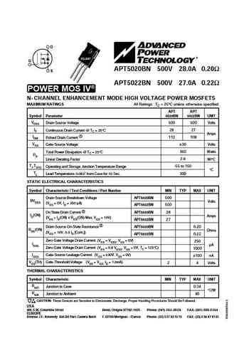
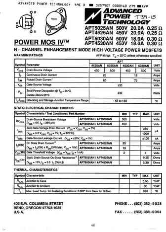
D TO-247 G APT5020BN 500V 28.0A 0.20 S APT5022BN 500V 27.0A 0.22 POWER MOS IV N- CHANNEL ENHANCEMENT MODE HIGH VOLTAGE POWER MOSFETS MAXIMUM RATINGS All Ratings TC = 25 C unless otherwise specified. APT APT Symbol Parameter 5020BN 5022BN UNIT VDSS Drain-Source Voltage 500 500 Volts ID Continuous Drain Current @ TC = 25 C 28 27 Amps IDM Pulsed Drain Current 1 112 108
7.1. Size:58K apt
apt5022avr.pdf

APT5022AVR 500V 21A 0.220 POWER MOS V TO-3 Power MOS V is a new generation of high voltage N-Channel enhancement mode power MOSFETs. This new technology minimizes the JFET effect, increases packing density and reduces the on-resistance. Power MOS V also achieves faster switching speeds through optimized gate layout. D Faster Switching 100% Avalanche Tested Lower L
8.1. Size:65K apt
apt5028svr.pdf
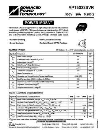
APT5028SVR 500V 20A 0.280 POWER MOS V D3PAK Power MOS V is a new generation of high voltage N-Channel enhancement mode power MOSFETs. This new technology minimizes the JFET effect, increases packing density and reduces the on-resistance. Power MOS V also achieves faster switching speeds through optimized gate layout. Faster Switching 100% Avalanche Tested D Lower L
8.2. Size:71K apt
apt5024bfll.pdf
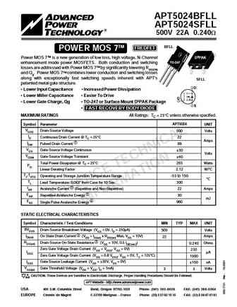
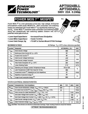
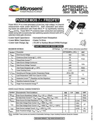
APT5024BFLL APT5024SFLL 500V 22A 0.240W TM BFLL FREDFET POWER MOS 7 Power MOS 7TM is a new generation of low loss, high voltage, N-Channel D3PAK TO-247 enhancement mode power MOSFETS. Both conduction and switching losses are addressed with Power MOS 7TM by significantly lowering RDS(ON) and Qg. Power MOS 7TM combines lower conduction and switching losses along with exceptionally fas
8.4. Size:170K apt
apt5024bll apt5024sll.pdf
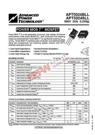
APT5024BLL APT5024SLL 500V 22A 0.240 R BLL POWER MOS 7 MOSFET D3PAK Power MOS 7 is a new generation of low loss, high voltage, N-Channel TO-247 enhancement mode power MOSFETS. Both conduction and switching losses are addressed with Power MOS 7 by significantly lowering RDS(ON) and Qg. Power MOS 7 combines lower conduction and switching losses SLL along
8.5. Size:32K apt
apt5024svr.pdf
APT5024SVR 500V 22A 0.240 POWER MOS V Power MOS V is a new generation of high voltage N-Channel enhancement D3PAK mode power MOSFETs. This new technology minimizes the JFET effect, increases packing density and reduces the on-resistance. Power MOS V also achieves faster switching speeds through optimized gate layout. Faster Switching 100% Avalanche Tested D Lower Leak
8.6. Size:59K apt
apt5026hvr.pdf
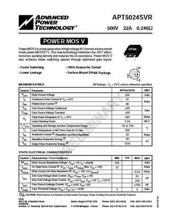
APT5026HVR 500V 18.5A 0.260 POWER MOS V TO-258 Power MOS V is a new generation of high voltage N-Channel enhancement mode power MOSFETs. This new technology minimizes the JFET effect, increases packing density and reduces the on-resistance. Power MOS V also achieves faster switching speeds through optimized gate layout. Faster Switching 100% Avalanche Tested D Lowe
8.7. Size:51K apt
apt5025bn.pdf

D TO-247 G APT5025BN 500V 23.0A 0.25 S APT5030BN 500V 21.0A 0.30 POWER MOS IV N- CHANNEL ENHANCEMENT MODE HIGH VOLTAGE POWER MOSFETS MAXIMUM RATINGS All Ratings TC = 25 C unless otherwise specified. APT APT Symbol Parameter 5025BN 5030BN UNIT VDSS Drain-Source Voltage 500 500 Volts ID Continuous Drain Current @ TC = 25 C 23 21 Amps IDM Pulsed Drain Current 1 92 84 V
8.8. Size:62K apt
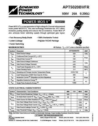
apt5020svr.pdf
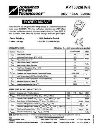
APT5020SVR 500V 26A 0.200 POWER MOS V Power MOS V is a new generation of high voltage N-Channel enhancement D3PAK mode power MOSFETs. This new technology minimizes the JFET effect, increases packing density and reduces the on-resistance. Power MOS V also achieves faster switching speeds through optimized gate layout. Faster Switching 100% Avalanche Tested D Lower Le
8.9. Size:51K apt
apt5020bn.pdf
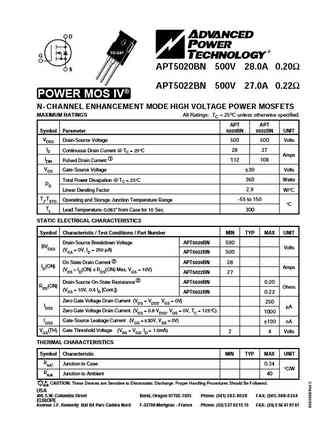
D TO-247 G APT5020BN 500V 28.0A 0.20 S APT5022BN 500V 27.0A 0.22 POWER MOS IV N- CHANNEL ENHANCEMENT MODE HIGH VOLTAGE POWER MOSFETS MAXIMUM RATINGS All Ratings TC = 25 C unless otherwise specified. APT APT Symbol Parameter 5020BN 5022BN UNIT VDSS Drain-Source Voltage 500 500 Volts ID Continuous Drain Current @ TC = 25 C 28 27 Amps IDM Pulsed Drain Current 1 112 108
8.10. Size:96K apt
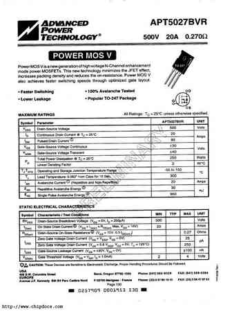
apt5027.pdf
http //www.chipdocs.com http //www.chipdocs.com
8.11. Size:59K apt
apt5024bvr.pdf

APT5024BVR 500V 22A 0.240 POWER MOS V Power MOS V is a new generation of high voltage N-Channel enhancement TO-247 mode power MOSFETs. This new technology minimizes the JFET effect, increases packing density and reduces the on-resistance. Power MOS V also achieves faster switching speeds through optimized gate layout. Faster Switching 100% Avalanche Tested D Lower L
8.12. Size:62K apt
apt5028bvr.pdf
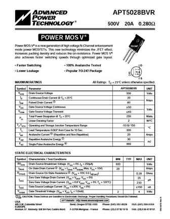
APT5028BVR 500V 20A 0.280 POWER MOS V Power MOS V is a new generation of high voltage N-Channel enhancement TO-247 mode power MOSFETs. This new technology minimizes the JFET effect, increases packing density and reduces the on-resistance. Power MOS V also achieves faster switching speeds through optimized gate layout. Faster Switching 100% Avalanche Tested D Lower L
8.13. Size:61K apt
apt5020bvfr.pdf
APT5020BVFR 500V 26A 0.200 POWER MOS V FREDFET Power MOS V is a new generation of high voltage N-Channel enhancement TO-247 mode power MOSFETs. This new technology minimizes the JFET effect, increases packing density and reduces the on-resistance. Power MOS V also achieves faster switching speeds through optimized gate layout. Fast Recovery Body Diode 100% Avalanche Test
8.14. Size:64K apt
apt5020svfr.pdf
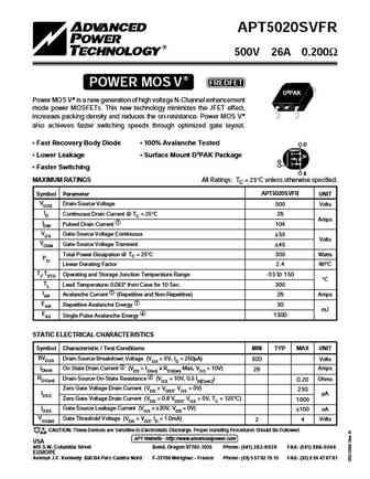
APT5020SVFR 500V 26A 0.200 POWER MOS V FREDFET D3PAK Power MOS V is a new generation of high voltage N-Channel enhancement mode power MOSFETs. This new technology minimizes the JFET effect, increases packing density and reduces the on-resistance. Power MOS V also achieves faster switching speeds through optimized gate layout. Fast Recovery Body Diode 100% Avalanche Test
8.15. Size:113K apt
apt5024svfrg.pdf
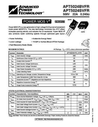
APT5024BVFR APT5024SVFR 500V 22A 0.240 BVFR FREDFET POWER MOS V D3PAK TO-247 Power MOS V is a new generation of high voltage N-Channel enhancement mode power MOSFETs. This new technology minimizes the JFET effect, increases packing density and reduces the on-resistance. Power MOS V SVFR also achieves faster switching speeds through optimized gate layout.
8.16. Size:34K apt
apt5020blc.pdf
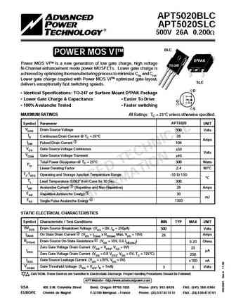
APT5020BLC APT5020SLC 500V 26A 0.200W BLC TM POWER MOS VI D3PAK Power MOS VITM is a new generation of low gate charge, high voltage TO-247 N-Channel enhancement mode power MOSFETs. Lower gate charge is achieved by optimizing the manufacturing process to minimize Ciss and Crss. Lower gate charge coupled with Power MOS VITM optimized gate layout, SLC delivers exceptionally fast switc
8.17. Size:59K apt
apt5020bvr.pdf

APT5020BVR 500V 26A 0.200 POWER MOS V Power MOS V is a new generation of high voltage N-Channel enhancement TO-247 mode power MOSFETs. This new technology minimizes the JFET effect, increases packing density and reduces the on-resistance. Power MOS V also achieves faster switching speeds through optimized gate layout. Faster Switching 100% Avalanche Tested D Lower L
8.18. Size:162K apt
apt5024bllg.pdf
APT5024BLL APT5024SLL 500V 22A 0.240 R BLL POWER MOS 7 MOSFET D3PAK Power MOS 7 is a new generation of low loss, high voltage, N-Channel TO-247 enhancement mode power MOSFETS. Both conduction and switching losses are addressed with Power MOS 7 by significantly lowering RDS(ON) and Qg. Power MOS 7 combines lower conduction and switching losses SLL along
8.19. Size:61K apt
apt5024bvfr.pdf

APT5024BVFR 500V 22A 0.240 POWER MOS V FREDFET Power MOS V is a new generation of high voltage N-Channel enhancement TO-247 mode power MOSFETs. This new technology minimizes the JFET effect, increases packing density and reduces the on-resistance. Power MOS V also achieves faster switching speeds through optimized gate layout. Fast Recovery Body Diode 100% Avalanche Tes
8.20. Size:60K apt
apt5024avr.pdf
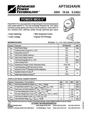
APT5024AVR 500V 18.5A 0.240 POWER MOS V TO-3 Power MOS V is a new generation of high voltage N-Channel enhancement mode power MOSFETs. This new technology minimizes the JFET effect, increases packing density and reduces the on-resistance. Power MOS V also achieves faster switching speeds through optimized gate layout. D Faster Switching 100% Avalanche Tested Lower
8.21. Size:62K apt
apt5020.pdf

APT5020SVR 500V 26A 0.200 POWER MOS V Power MOS V is a new generation of high voltage N-Channel enhancement D3PAK mode power MOSFETs. This new technology minimizes the JFET effect, increases packing density and reduces the on-resistance. Power MOS V also achieves faster switching speeds through optimized gate layout. Faster Switching 100% Avalanche Tested D Lower Le
8.22. Size:216K microsemi
apt5024sfll apt5024sfllg.pdf
APT5024BFLL APT5024SFLL 500V 22A 0.240 BFLL R POWER MOS 7 FREDFET (B) Power MOS 7 is a new generation of low loss, high voltage, N-Channel D3PAK enhancement mode power MOSFETS. Both conduction and switch- (S) ing losses are addressed with Power MOS 7 by significantly lowering C G E RDS(ON) and Qg. Power MOS 7 combines lower conduction and switching losses along wi
8.23. Size:375K inchange semiconductor
apt5024bfll.pdf

isc N-Channel MOSFET Transistor APT5024BFLL FEATURES Drain Current I =22A@ T =25 D C Drain Source Voltage- V =500V(Min) DSS Static Drain-Source On-Resistance R =0.24 (Max) DS(on) 100% avalanche tested Minimum Lot-to-Lot variations for robust device performance and reliable operation DESCRIPTION Designed for use in switch mode power supplies and general purp
8.24. Size:375K inchange semiconductor
apt5024bvr.pdf

isc N-Channel MOSFET Transistor APT5024BVR FEATURES Drain Current I =22A@ T =25 D C Drain Source Voltage- V =500V(Min) DSS Static Drain-Source On-Resistance R =0.24 (Max) DS(on) 100% avalanche tested Minimum Lot-to-Lot variations for robust device performance and reliable operation DESCRIPTION Designed for use in switch mode power supplies and general purpo
8.25. Size:375K inchange semiconductor
apt5028bvr.pdf
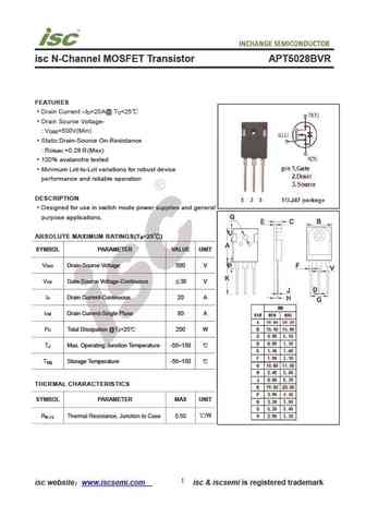
isc N-Channel MOSFET Transistor APT5028BVR FEATURES Drain Current I =20A@ T =25 D C Drain Source Voltage- V =500V(Min) DSS Static Drain-Source On-Resistance R =0.28 (Max) DS(on) 100% avalanche tested Minimum Lot-to-Lot variations for robust device performance and reliable operation DESCRIPTION Designed for use in switch mode power supplies and general purpo
8.26. Size:375K inchange semiconductor
apt5020bvfr.pdf
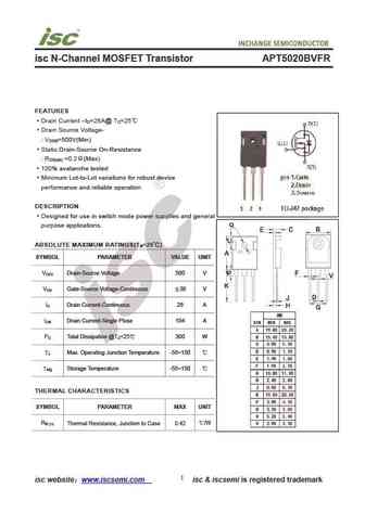
isc N-Channel MOSFET Transistor APT5020BVFR FEATURES Drain Current I =26A@ T =25 D C Drain Source Voltage- V =500V(Min) DSS Static Drain-Source On-Resistance R =0.2 (Max) DS(on) 100% avalanche tested Minimum Lot-to-Lot variations for robust device performance and reliable operation DESCRIPTION Designed for use in switch mode power supplies and general purpo
8.27. Size:375K inchange semiconductor
apt5024bll.pdf

isc N-Channel MOSFET Transistor APT5024BLL FEATURES Drain Current I =22A@ T =25 D C Drain Source Voltage- V =500V(Min) DSS Static Drain-Source On-Resistance R =0.24 (Max) DS(on) 100% avalanche tested Minimum Lot-to-Lot variations for robust device performance and reliable operation DESCRIPTION Designed for use in switch mode power supplies and general purpo
8.28. Size:375K inchange semiconductor
apt5020bvr.pdf

isc N-Channel MOSFET Transistor APT5020BVR FEATURES Drain Current I =26A@ T =25 D C Drain Source Voltage- V =500V(Min) DSS Static Drain-Source On-Resistance R =0.2 (Max) DS(on) 100% avalanche tested Minimum Lot-to-Lot variations for robust device performance and reliable operation DESCRIPTION Designed for use in switch mode power supplies and general purpos
8.29. Size:375K inchange semiconductor
apt5024bvfr.pdf

isc N-Channel MOSFET Transistor APT5024BVFR FEATURES Drain Current I =22A@ T =25 D C Drain Source Voltage- V =500V(Min) DSS Static Drain-Source On-Resistance R =0.24 (Max) DS(on) 100% avalanche tested Minimum Lot-to-Lot variations for robust device performance and reliable operation DESCRIPTION Designed for use in switch mode power supplies and general purp
Otros transistores... 2SK4027
, APT5016BFLLG
, APT5016BLLG
, APT5016SFLLG
, APT5017SVFRG
, APT5018BFLLG
, APT5018SFLLG
, APT5018SLL
, IRF830
, APT5024BLL
, APT5024BLLG
, APT5024SFLL
, APT5024SFLLG
, APT5024SLL
, APT5024SVFRG
, APT5025AN
, APT5030AN
.