APT6025BLLG Datasheet. Equivalente. Reemplazo. Hoja de especificaciones. Principales características
Número de Parte: APT6025BLLG 📄📄
Tipo de FET: MOFETS
Polaridad de transistor: N
ESPECIFICACIONES MÁXIMAS
Pdⓘ - Máxima disipación de potencia: 325 W
|Vds|ⓘ - Voltaje máximo drenador-fuente: 600 V
|Vgs|ⓘ - Voltaje máximo fuente-puerta: 30 V
|Id|ⓘ - Corriente continua de drenaje: 24 A
Tjⓘ - Temperatura máxima de unión: 150 °C
CARACTERÍSTICAS ELÉCTRICAS
trⓘ - Tiempo de subida: 19 nS
Cossⓘ - Capacitancia de salida: 535 pF
RDSonⓘ - Resistencia estado encendido drenaje a fuente: 0.25 Ohm
Encapsulados: TO-247
📄📄 Copiar
Búsqueda de reemplazo de APT6025BLLG MOSFET
- Selecciónⓘ de transistores por parámetros
APT6025BLLG datasheet
apt6025bllg.pdf
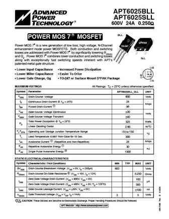
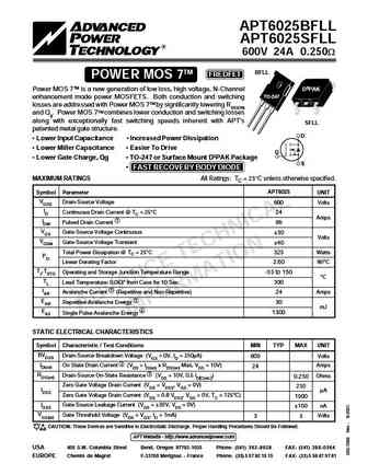
APT6025BLL APT6025SLL 600V 24A 0.250 R BLL POWER MOS 7 MOSFET D3PAK Power MOS 7 is a new generation of low loss, high voltage, N-Channel TO-247 enhancement mode power MOSFETS. Both conduction and switching losses are addressed with Power MOS 7 by significantly lowering RDS(ON) and Qg. Power MOS 7 combines lower conduction and switching losses SLL along
apt6025bll.pdf
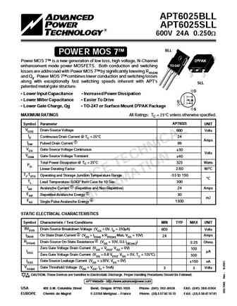
APT6025BLL APT6025SLL 600V 24A 0.250W TM BLL POWER MOS 7 Power MOS 7TM is a new generation of low loss, high voltage, N-Channel D3PAK TO-247 enhancement mode power MOSFETS. Both conduction and switching losses are addressed with Power MOS 7TM by significantly lowering RDS(ON) and Qg. Power MOS 7TM combines lower conduction and switching losses along with exceptionally fast switching
apt6025bll.pdf
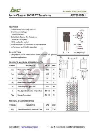
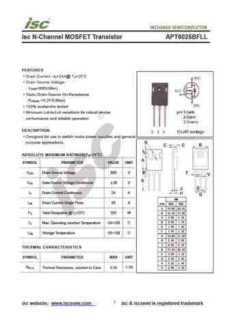
isc N-Channel MOSFET Transistor APT6025BLL FEATURES Drain Current I =24A@ T =25 D C Drain Source Voltage- V =600V(Min) DSS Static Drain-Source On-Resistance R =0.25 (Max) DS(on) 100% avalanche tested Minimum Lot-to-Lot variations for robust device performance and reliable operation DESCRIPTION Designed for use in switch mode power supplies and general purpo
apt6025bfllg apt6025sfllg.pdf
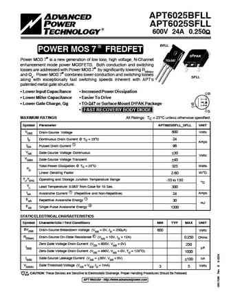
APT6025BFLL APT6025SFLL 600V 24A 0.250 BFLL R POWER MOS 7 FREDFET D3PAK Power MOS 7 is a new generation of low loss, high voltage, N-Channel TO-247 enhancement mode power MOSFETS. Both conduction and switching losses are addressed with Power MOS 7 by significantly lowering RDS(ON) and Qg. Power MOS 7 combines lower conduction and switching losses SFLL


Otros transistores... APT6017B2LLG, APT6017LFLLG, APT6017LLLG, APT6018JN, APT6021BFLLG, APT6021BLLG, APT6021SFLLG, APT6025BFLLG, IRFP450, APT6025BVFRG, APT6025BVRG, APT6025SFLLG, APT6025SVFRG, APT6029BFLLG, APT6029SFLLG, APT6029SLL, APT6029SLLG
Parámetros del MOSFET. Cómo se afectan entre sí.
History: J270 | PZF010HK | 2SK216
🌐 : EN ES РУ

Liste
Recientemente añadidas las descripciónes de los transistores:
MOSFET: CS95118 | CS85105A | CS75N45 | CS72N12 | CS55N50 | CS48N75A | CS40N27 | MSQ60P04D | MSQ40P07D | MSQ30P40D | MSQ30P15 | MSQ30P07D | MSQ100N03D | MSHM60P14 | MSHM40N085 | MSHM30N46
Popular searches
2n3394 | 2sb688 | 2sd551 | ac128 datasheet | 2n5496 | 2sb600 | 2sa1209 | 2sc1364 replacement