NTD4970N-1G MOSFET Equivalente. Reemplazo. Hoja de especificaciones. Principales características
Número de Parte: NTD4970N-1G
Tipo de FET: MOSFET
Polaridad de transistor: N
ESPECIFICACIONES MÁXIMAS
Pdⓘ - Máxima
disipación de potencia: 24.6 W
|Vds|ⓘ - Voltaje máximo drenador-fuente: 30 V
|Vgs|ⓘ - Voltaje máximo fuente-puerta: 20 V
|Id|ⓘ - Corriente continua
de drenaje: 36 A
Tjⓘ - Temperatura máxima de unión: 175 °C
CARACTERÍSTICAS ELÉCTRICAS
trⓘ - Tiempo
de subida: 27.6 nS
Cossⓘ - Capacitancia de salida: 306 pF
RDSonⓘ - Resistencia estado encendido drenaje a fuente: 0.011 Ohm
Encapsulados: DPAK
IPAK
Búsqueda de reemplazo de NTD4970N-1G MOSFET
- Selecciónⓘ de transistores por parámetros
NTD4970N-1G datasheet
..1. Size:113K onsemi
ntd4970n-1g.pdf 

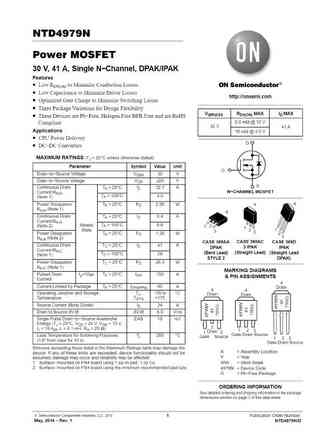
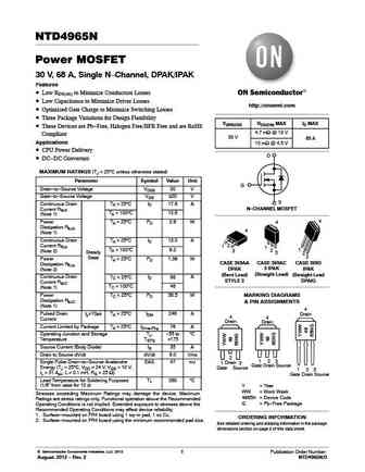
NTD4970N Power MOSFET 30 V, 36 A, Single N-Channel, DPAK/IPAK Features Low RDS(on) to Minimize Conduction Losses Low Capacitance to Minimize Driver Losses Optimized Gate Charge to Minimize Switching Losses http //onsemi.com Three Package Variations for Design Flexibility These Devices are Pb-Free, Halogen Free/BFR Free and are RoHS V(BR)DSS RDS(ON) MAX ID MAX Compl
6.1. Size:140K onsemi
ntd4970n.pdf
NTD4970N Power MOSFET 30 V, 36 A, Single N-Channel, DPAK/IPAK Features Low RDS(on) to Minimize Conduction Losses Low Capacitance to Minimize Driver Losses Optimized Gate Charge to Minimize Switching Losses http //onsemi.com Three Package Variations for Design Flexibility These Devices are Pb-Free, Halogen Free/BFR Free and are RoHS V(BR)DSS RDS(ON) MAX ID MAX Compl
9.1. Size:123K 1
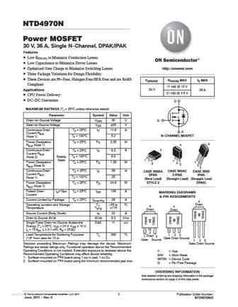
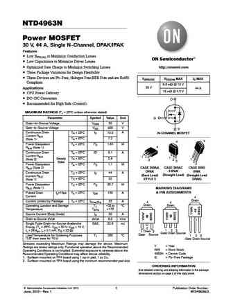
ntd4963ng.pdf
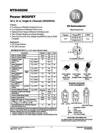
NTD4963N Power MOSFET 30 V, 44 A, Single N-Channel, DPAK/IPAK Features Low RDS(on) to Minimize Conduction Losses Low Capacitance to Minimize Driver Losses http //onsemi.com Optimized Gate Charge to Minimize Switching Losses Three Package Variations for Design Flexibility V(BR)DSS RDS(ON) MAX ID MAX These Devices are Pb-Free, Halogen Free/BFR Free and are RoHS 9.6
9.2. Size:86K onsemi
ntd4904n.pdf
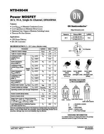
NTD4904N Power MOSFET 30 V, 79 A, Single N-Channel, DPAK/IPAK Features Low RDS(on) to Minimize Conduction Losses Low Capacitance to Minimize Driver Losses http //onsemi.com Optimized Gate Charge to Minimize Switching Losses These are Pb-Free Devices V(BR)DSS RDS(on) MAX ID MAX Applications 3.7 mW @ 10 V 30 V 79 A 5.5 mW @ 4.5 V CPU Power Delivery DC-DC Conv
9.3. Size:123K onsemi
ntd4906n.pdf
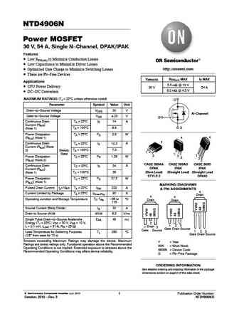
NTD4906N Power MOSFET 30 V, 54 A, Single N-Channel, DPAK/IPAK Features Low RDS(on) to Minimize Conduction Losses Low Capacitance to Minimize Driver Losses http //onsemi.com Optimized Gate Charge to Minimize Switching Losses These are Pb-Free Devices V(BR)DSS RDS(on) MAX ID MAX Applications 5.5 mW @ 10 V CPU Power Delivery 30 V 54 A 8.0 mW @ 4.5 V DC-DC Con
9.4. Size:118K onsemi
ntd4969n-d.pdf

NTD4969N Power MOSFET 30 V, 41 A, Single N-Channel, DPAK/IPAK Features Low RDS(on) to Minimize Conduction Losses Low Capacitance to Minimize Driver Losses http //onsemi.com Optimized Gate Charge to Minimize Switching Losses Three Package Variations for Design Flexibility V(BR)DSS RDS(ON) MAX ID MAX These Devices are Pb-Free, Halogen Free/BFR Free and are RoHS 9.0
9.5. Size:114K onsemi
ntd4969n-1g.pdf
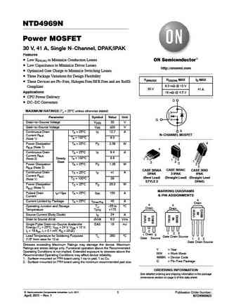
NTD4969N Power MOSFET 30 V, 41 A, Single N-Channel, DPAK/IPAK Features Low RDS(on) to Minimize Conduction Losses Low Capacitance to Minimize Driver Losses http //onsemi.com Optimized Gate Charge to Minimize Switching Losses Three Package Variations for Design Flexibility V(BR)DSS RDS(ON) MAX ID MAX These Devices are Pb-Free, Halogen Free/BFR Free and are RoHS 9.0
9.6. Size:82K onsemi
ntd4969n.pdf
NTD4969N Power MOSFET 30 V, 41 A, Single N-Channel, DPAK/IPAK Features Low RDS(on) to Minimize Conduction Losses Low Capacitance to Minimize Driver Losses http //onsemi.com Optimized Gate Charge to Minimize Switching Losses Three Package Variations for Design Flexibility V(BR)DSS RDS(ON) MAX ID MAX These Devices are Pb-Free, Halogen Free/BFR Free and are RoHS 9.0
9.7. Size:115K onsemi
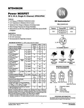
ntd4963n-1g.pdf
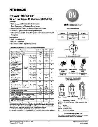
NTD4963N Power MOSFET 30 V, 44 A, Single N-Channel, DPAK/IPAK Features Low RDS(on) to Minimize Conduction Losses Low Capacitance to Minimize Driver Losses Optimized Gate Charge to Minimize Switching Losses http //onsemi.com Three Package Variations for Design Flexibility These Devices are Pb-Free, Halogen Free/BFR Free and are RoHS V(BR)DSS RDS(ON) MAX ID MAX Compl
9.8. Size:141K onsemi
ntd4904n-1g ntd4904n.pdf
NTD4904N Power MOSFET 30 V, 79 A, Single N-Channel, DPAK/IPAK Features Low RDS(on) to Minimize Conduction Losses Low Capacitance to Minimize Driver Losses http //onsemi.com Optimized Gate Charge to Minimize Switching Losses These are Pb-Free Devices V(BR)DSS RDS(on) MAX ID MAX Applications 3.7 mW @ 10 V 30 V 79 A 5.5 mW @ 4.5 V CPU Power Delivery DC-DC Conv
9.9. Size:112K onsemi
ntd4965n-d.pdf
NTD4965N Power MOSFET 30 V, 68 A, Single N-Channel, DPAK/IPAK Features Low RDS(on) to Minimize Conduction Losses Low Capacitance to Minimize Driver Losses http //onsemi.com Optimized Gate Charge to Minimize Switching Losses Three Package Variations for Design Flexibility V(BR)DSS RDS(ON) MAX ID MAX These Devices are Pb-Free, Halogen Free/BFR Free and are RoHS 4.7
9.10. Size:140K onsemi
ntd4913n.pdf
NTD4913N Power MOSFET 30 V, 32 A, Single N-Channel, DPAK/IPAK Features Low RDS(on) to Minimize Conduction Losses Low Capacitance to Minimize Driver Losses http //onsemi.com Optimized Gate Charge to Minimize Switching Losses These are Pb-Free Devices V(BR)DSS RDS(ON) MAX ID MAX Applications 10.5 mW @ 10 V CPU Power Delivery 30 V 32 A 15 mW @ 4.5 V DC-DC Con
9.11. Size:138K onsemi
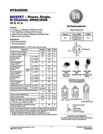
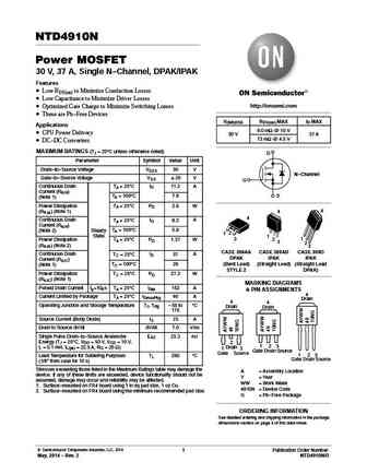
ntd4910n-1g.pdf

NTD4910N Power MOSFET 30 V, 37 A, Single N-Channel, DPAK/IPAK Features Low RDS(on) to Minimize Conduction Losses Low Capacitance to Minimize Driver Losses http //onsemi.com Optimized Gate Charge to Minimize Switching Losses These are Pb-Free Devices V(BR)DSS RDS(on) MAX ID MAX Applications 9.0 mW @ 10 V CPU Power Delivery 30 V 37 A 13 mW @ 4.5 V DC-DC Conv
9.12. Size:138K onsemi
ntd4960n-1g.pdf
NTD4960N Power MOSFET 30 V, 55 A, Single N-Channel, DPAK/IPAK Features Low RDS(on) to Minimize Conduction Losses Low Capacitance to Minimize Driver Losses http //onsemi.com Optimized Gate Charge to Minimize Switching Losses Three Package Variations for Design Flexibility V(BR)DSS RDS(ON) MAX ID MAX These Devices are Pb-Free, Halogen Free/BFR Free and are RoHS 8.0
9.13. Size:107K onsemi
ntd4965n-1g.pdf
NTD4965N Power MOSFET 30 V, 68 A, Single N-Channel, DPAK/IPAK Features Low RDS(on) to Minimize Conduction Losses Low Capacitance to Minimize Driver Losses http //onsemi.com Optimized Gate Charge to Minimize Switching Losses Three Package Variations for Design Flexibility V(BR)DSS RDS(ON) MAX ID MAX These Devices are Pb-Free, Halogen Free/BFR Free and are RoHS 4.7
9.14. Size:138K onsemi
ntd4909n-1g ntd4909n.pdf
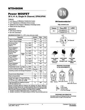
NTD4909N Power MOSFET 30 V, 41 A, Single N-Channel, DPAK/IPAK Features Low RDS(on) to Minimize Conduction Losses Low Capacitance to Minimize Driver Losses http //onsemi.com Optimized Gate Charge to Minimize Switching Losses These are Pb-Free Devices V(BR)DSS RDS(on) MAX ID MAX Applications 8.0 mW @ 10 V CPU Power Delivery 30 V 41 A 12 mW @ 4.5 V DC-DC Conv
9.15. Size:137K onsemi
ntd4909n.pdf
NTD4909N MOSFET Power, Single, N-Channel, DPAK/IPAK 30 V, 41 A Features Low RDS(on) to Minimize Conduction Losses http //onsemi.com Low Capacitance to Minimize Driver Losses Optimized Gate Charge to Minimize Switching Losses V(BR)DSS RDS(on) MAX ID MAX These are Pb-Free Devices 8.0 mW @ 10 V 30 V 41 A 12 mW @ 4.5 V Applications CPU Power Delivery D DC-
9.16. Size:108K onsemi
ntd4910n.pdf
NTD4910N Power MOSFET 30 V, 37 A, Single N-Channel, DPAK/IPAK Features Low RDS(on) to Minimize Conduction Losses Low Capacitance to Minimize Driver Losses http //onsemi.com Optimized Gate Charge to Minimize Switching Losses These are Pb-Free Devices V(BR)DSS RDS(on) MAX ID MAX Applications 9.0 mW @ 10 V CPU Power Delivery 30 V 37 A 13 mW @ 4.5 V DC-DC Conv
9.17. Size:139K onsemi
ntd4963n.pdf
NTD4963N Power MOSFET 30 V, 44 A, Single N-Channel, DPAK/IPAK Features Low RDS(on) to Minimize Conduction Losses Low Capacitance to Minimize Driver Losses Optimized Gate Charge to Minimize Switching Losses http //onsemi.com Three Package Variations for Design Flexibility These Devices are Pb-Free, Halogen Free/BFR Free and are RoHS V(BR)DSS RDS(ON) MAX ID MAX Compl
Otros transistores... NTD4865N-1G
, NTD4904N-1G
, NTD4909N-1G
, NTD4910N-1G
, NTD4960N-1G
, NTD4963N-1G
, NTD4965N-1G
, NTD4969N-1G
, IRF520
, NTD50N03R
, NTD5406NG
, NTD5407NG
, NTD5413NT4G
, NTD5414NT4G
, NTD5802NT4G
, NTD5804NT4G
, NTD5805NT4G
.
History: BSS7728NG
| WM05N03M
| WMS08DH04T1