NTLJS1102PTBG Datasheet. Equivalente. Reemplazo. Hoja de especificaciones. Principales características
Número de Parte: NTLJS1102PTBG 📄📄
Tipo de FET: MOSFET
Polaridad de transistor: P
ESPECIFICACIONES MÁXIMAS
Pdⓘ - Máxima disipación de potencia: 0.7 W
|Vds|ⓘ - Voltaje máximo drenador-fuente: 8 V
|Vgs|ⓘ - Voltaje máximo fuente-puerta: 6 V
|Id|ⓘ - Corriente continua de drenaje: 3.7 A
Tjⓘ - Temperatura máxima de unión: 150 °C
CARACTERÍSTICAS ELÉCTRICAS
trⓘ - Tiempo de subida: 41 nS
Cossⓘ - Capacitancia de salida: 350 pF
RDSonⓘ - Resistencia estado encendido drenaje a fuente: 0.036 Ohm
Encapsulados: WDFN6
📄📄 Copiar
Búsqueda de reemplazo de NTLJS1102PTBG MOSFET
- Selecciónⓘ de transistores por parámetros
NTLJS1102PTBG datasheet
ntljs1102p ntljs1102ptag ntljs1102ptbg.pdf
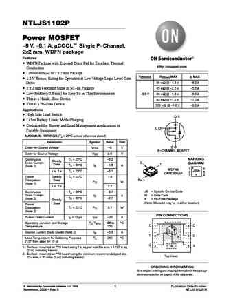
NTLJS1102P Power MOSFET -8 V, -8.1 A, mCOOL] Single P-Channel, 2x2 mm, WDFN package Features WDFN Package with Exposed Drain Pad for Excellent Thermal http //onsemi.com Conduction Lowest RDS(on) in 2 x 2 mm Package V(BR)DSS RDS(on) MAX ID MAX 1.2 V RDS(on) Rating for Operation at Low Voltage Logic Level Gate 36 mW @ -4.5 V -6.2 A Drive 2 x 2 mm Footprint Same as SC-
ntljs17d0p03p8z.pdf
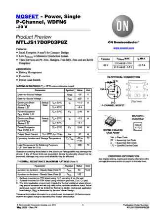
MOSFET - Power, Single P-Channel, WDFN6 -30 V Product Preview NTLJS17D0P03P8Z www.onsemi.com Features Small Footprint (4 mm2) for Compact Design Low RDS(on) to Minimize Conduction Losses V(BR)DSS RDS(on) MAX ID MAX These Devices are Pb-Free, Halogen-Free/BFR-Free and are RoHS Compliant 11.3 mW @ -10 V -30 V -11.7 A 21.3 mW @ -4.5 V Applications Battery Management
ntljs4114n.pdf

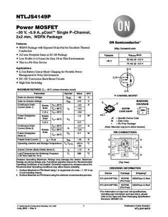
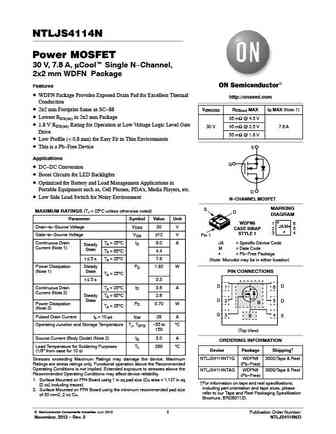
NTLJS4114N Power MOSFET 30 V, 7.8 A, mCoolt Single N-Channel, 2x2 mm WDFN Package Features WDFN Package Provides Exposed Drain Pad for Excellent Thermal http //onsemi.com Conduction 2x2 mm Footprint Same as SC-88 V(BR)DSS RDS(on) MAX ID MAX (Note 1) Lowest RDS(on) in 2x2 mm Package 35 mW @ 4.5 V 1.8 V RDS(on) Rating for Operation at Low Voltage Logic Level Gate 30 V
ntljs3180pz ntljs3180pztbg.pdf
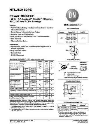
NTLJS3180PZ Power MOSFET -20 V, -7.7 A, mCoolt Single P-Channel, ESD, 2x2 mm WDFN Package Features WDFN 2x2 mm Package with Exposed Drain Pads for Excellent http //onsemi.com Thermal Conduction Lowest RDS(on) Solution in 2x2 mm Package V(BR)DSS RDS(on) MAX ID MAX Footprint Same as SC-88 Package 38 mW @ -4.5 V Low Profile (


Otros transistores... NTLJD3182FZTAG, NTLJD3182FZTBG, NTLJF3117PT1G, NTLJF3117PTAG, NTLJF3118NTAG, NTLJF4156NT1G, NTLJF4156NTAG, NTLJS1102PTAG, IRF640N, NTLJS2103PTAG, NTLJS2103PTBG, NTLJS3113PT1G, NTLJS3113PTAG, NTLJS3180PZTBG, NTLJS3A18PZ, NTLJS4114NT1G, NTLJS4149PTAG
History: NTGS3441BT1G
🌐 : EN ES РУ

Liste
Recientemente añadidas las descripciónes de los transistores:
MOSFET: BCD70N07A | BCD90N03 | BCD80N06 | T50N06 | H50N06 | BCD12N65 | BCT12N65 | BCD4N65 | BCT4N65 | BCD7N65 | BCT7N65 | BCT20N65 | ASDM30P100KQ | ASDM30N90Q | ASDM30N75KQ | ASDM30N150Q
Popular searches
ksc2383 datasheet | 2n3906 equivalent | a733 transistor equivalent | 2n5401 transistor datasheet | 2n2222 data sheet | irf3205 datasheet | oc71 | njw0302g