NTMFS4C09NT1G Datasheet. Equivalente. Reemplazo. Hoja de especificaciones. Principales características
Número de Parte: NTMFS4C09NT1G 📄📄
Código: 4C09N
Tipo de FET: MOSFET
Polaridad de transistor: N
ESPECIFICACIONES MÁXIMAS
Pdⓘ - Máxima disipación de potencia: 0.76 W
|Vds|ⓘ - Voltaje máximo drenador-fuente: 30 V
|Vgs|ⓘ - Voltaje máximo fuente-puerta: 20 V
|Id|ⓘ - Corriente continua de drenaje: 9 A
Tjⓘ - Temperatura máxima de unión: 150 °C
CARACTERÍSTICAS ELÉCTRICAS
|VGSth|ⓘ - Tensión umbral entre puerta y fuente: 2.1 V
Qgⓘ - Carga de la puerta: 10.9 nC
trⓘ - Tiempo de subida: 32 nS
Cossⓘ - Capacitancia de salida: 610 pF
RDSonⓘ - Resistencia estado encendido drenaje a fuente: 0.0058 Ohm
Encapsulados: SO-8FL
📄📄 Copiar
Búsqueda de reemplazo de NTMFS4C09NT1G MOSFET
- Selecciónⓘ de transistores por parámetros
NTMFS4C09NT1G datasheet
..1. Size:93K onsemi
ntmfs4c09nt1g.pdf 

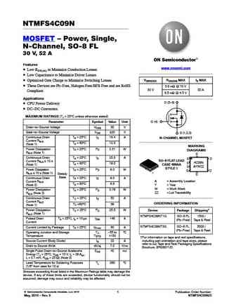
NTMFS4C09N Power MOSFET 30 V, 52 A, Single N-Channel, SO-8 FL Features Low RDS(on) to Minimize Conduction Losses Low Capacitance to Minimize Driver Losses www.onsemi.com Optimized Gate Charge to Minimize Switching Losses These Devices are Pb-Free, Halogen Free/BFR Free and are RoHS V(BR)DSS RDS(ON) MAX ID MAX Compliant 5.8 mW @ 10 V Applications 30 V 52 A 8.5 mW @
4.1. Size:140K onsemi
ntmfs4c09n.pdf 

NTMFS4C09N MOSFET Power, Single, N-Channel, SO-8 FL 30 V, 52 A Features www.onsemi.com Low RDS(on) to Minimize Conduction Losses Low Capacitance to Minimize Driver Losses V(BR)DSS RDS(ON) MAX ID MAX Optimized Gate Charge to Minimize Switching Losses These Devices are Pb-Free, Halogen Free/BFR Free and are RoHS 5.8 mW @ 10 V 30 V 52 A Compliant 8.5 mW @ 4.5 V A
6.1. Size:138K 1
ntmfs4c06n.pdf 

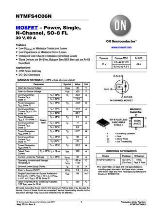
NTMFS4C06N MOSFET Power, Single, N-Channel, SO-8 FL 30 V, 69 A Features www.onsemi.com Low RDS(on) to Minimize Conduction Losses Low Capacitance to Minimize Driver Losses Optimized Gate Charge to Minimize Switching Losses V(BR)DSS RDS(ON) MAX ID MAX These Devices are Pb-Free, Halogen Free/BFR Free and are RoHS 4.0 mW @ 10 V Compliant 30 V 69 A 6.0 mW @ 4.5 V A
6.2. Size:79K 1
ntmfs4c05nt1g.pdf 

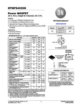
NTMFS4C05N Power MOSFET 30 V, 78 A, Single N-Channel, SO-8 FL Features Low RDS(on) to Minimize Conduction Losses Low Capacitance to Minimize Driver Losses www.onsemi.com Optimized Gate Charge to Minimize Switching Losses These Devices are Pb-Free, Halogen Free/BFR Free and are RoHS Compliant V(BR)DSS RDS(ON) MAX ID MAX Applications 3.4 mW @ 10 V 30 V 78 A CPU P
6.3. Size:179K onsemi
ntmfs4c054n.pdf 

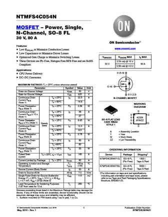
NTMFS4C054N MOSFET Power, Single, N-Channel, SO-8 FL 30 V, 80 A Features www.onsemi.com Low RDS(on) to Minimize Conduction Losses Low Capacitance to Minimize Driver Losses V(BR)DSS RDS(ON) MAX ID MAX Optimized Gate Charge to Minimize Switching Losses These Devices are Pb-Free, Halogen Free/BFR Free and are RoHS 2.54 mW @ 10 V 30 V 80 A Compliant 3.56 mW @ 4.5 V
6.4. Size:173K onsemi
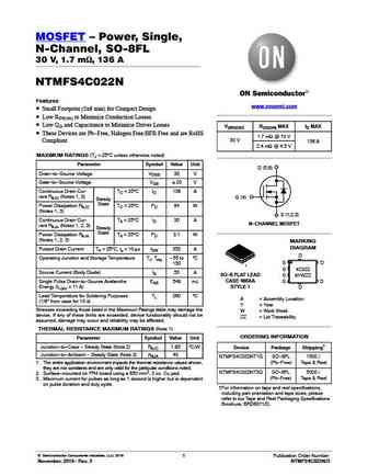
ntmfs4c022n.pdf 

MOSFET Power, Single, N-Channel, SO-8FL 30 V, 1.7 mW, 136 A NTMFS4C022N Features www.onsemi.com Small Footprint (5x6 mm) for Compact Design Low RDS(on) to Minimize Conduction Losses Low QG and Capacitance to Minimize Driver Losses V(BR)DSS RDS(ON) MAX ID MAX These Devices are Pb-Free, Halogen Free/BFR Free and are RoHS 1.7 mW @ 10 V 30 V Compliant 136 A 2.4 mW
6.5. Size:177K onsemi
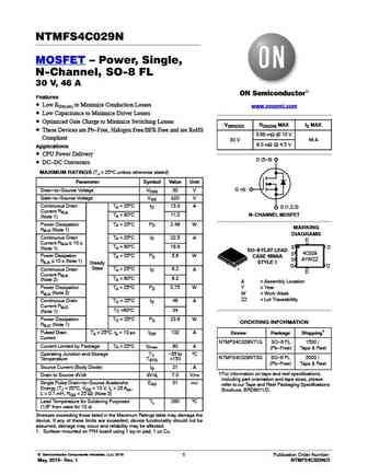
ntmfs4c029n.pdf 

NTMFS4C029N MOSFET Power, Single, N-Channel, SO-8 FL 30 V, 46 A Features Low RDS(on) to Minimize Conduction Losses www.onsemi.com Low Capacitance to Minimize Driver Losses Optimized Gate Charge to Minimize Switching Losses V(BR)DSS RDS(ON) MAX ID MAX These Devices are Pb-Free, Halogen Free/BFR Free and are RoHS 5.88 mW @ 10 V Compliant 30 V 46 A 9.0 mW @ 4.5 V
6.6. Size:84K onsemi
ntmfs4c05n.pdf 

NTMFS4C05N Power MOSFET 30 V, 78 A, Single N-Channel, SO-8 FL Features Low RDS(on) to Minimize Conduction Losses Low Capacitance to Minimize Driver Losses www.onsemi.com Optimized Gate Charge to Minimize Switching Losses These Devices are Pb-Free, Halogen Free/BFR Free and are RoHS Compliant V(BR)DSS RDS(ON) MAX ID MAX Applications 3.4 mW @ 10 V 30 V 78 A CPU P
6.7. Size:175K onsemi
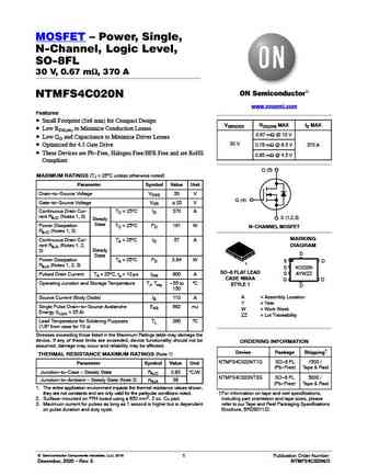
ntmfs4c020n.pdf 

MOSFET Power, Single, N-Channel, Logic Level, SO-8FL 30 V, 0.67 mW, 370 A NTMFS4C020N www.onsemi.com Features Small Footprint (5x6 mm) for Compact Design V(BR)DSS RDS(ON) MAX ID MAX Low RDS(on) to Minimize Conduction Losses 0.67 mW @ 10 V Low QG and Capacitance to Minimize Driver Losses 30 V 0.78 mW @ 6.5 V 370 A Optimized for 4.5 Gate Drive These Devices
6.8. Size:115K onsemi
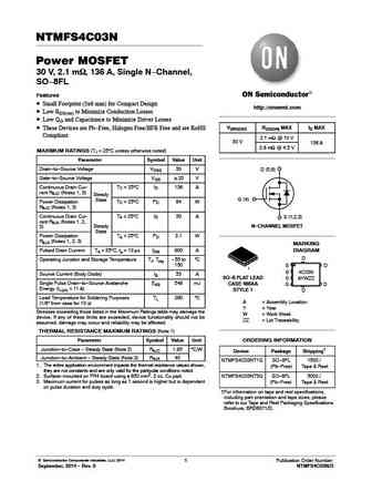
ntmfs4c03n.pdf 

NTMFS4C03N Power MOSFET 30 V, 2.1 mW, 136 A, Single N-Channel, SO-8FL Features Small Footprint (5x6 mm) for Compact Design http //onsemi.com Low RDS(on) to Minimize Conduction Losses Low QG and Capacitance to Minimize Driver Losses V(BR)DSS RDS(ON) MAX ID MAX These Devices are Pb-Free, Halogen Free/BFR Free and are RoHS Compliant 2.1 mW @ 10 V 30 V 136 A 2.8 mW @
6.9. Size:91K onsemi
ntmfs4c08n.pdf 

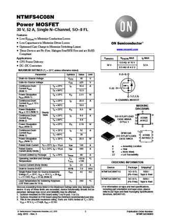
NTMFS4C08N Power MOSFET 30 V, 52 A, Single N-Channel, SO-8 FL Features Low RDS(on) to Minimize Conduction Losses Low Capacitance to Minimize Driver Losses Optimized Gate Charge to Minimize Switching Losses www.onsemi.com These Devices are Pb-Free, Halogen Free/BFR Free and are RoHS Compliant Applications V(BR)DSS RDS(ON) MAX ID MAX CPU Power Delivery 5.8 mW @ 10
6.10. Size:139K onsemi
ntmfs4c025n.pdf 

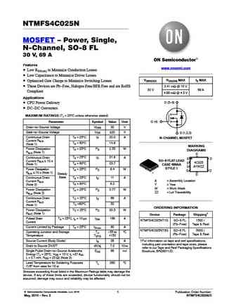
NTMFS4C025N MOSFET Power, Single, N-Channel, SO-8 FL 30 V, 69 A Features www.onsemi.com Low RDS(on) to Minimize Conduction Losses Low Capacitance to Minimize Driver Losses V(BR)DSS RDS(ON) MAX ID MAX Optimized Gate Charge to Minimize Switching Losses These Devices are Pb-Free, Halogen Free/BFR Free and are RoHS 3.41 mW @ 10 V 30 V 69 A Compliant 4.88 mW @ 4.5 V
6.11. Size:171K onsemi
ntmfs4c032n.pdf 

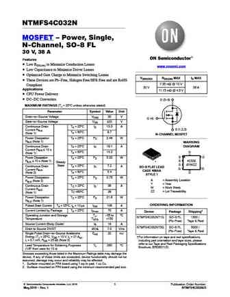
NTMFS4C032N MOSFET Power, Single, N-Channel, SO-8 FL 30 V, 38 A Features Low RDS(on) to Minimize Conduction Losses www.onsemi.com Low Capacitance to Minimize Driver Losses Optimized Gate Charge to Minimize Switching Losses V(BR)DSS RDS(ON) MAX ID MAX These Devices are Pb-Free, Halogen Free/BFR Free and are RoHS 7.35 mW @ 10 V Compliant 30 V 38 A Applications 1
6.12. Size:178K onsemi
ntmfs4c027n.pdf 

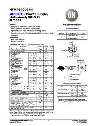
NTMFS4C027N MOSFET Power, Single, N-Channel, SO-8 FL 30 V, 52 A Features Low RDS(on) to Minimize Conduction Losses www.onsemi.com Low Capacitance to Minimize Driver Losses Optimized Gate Charge to Minimize Switching Losses These Devices are Pb-Free, Halogen Free/BFR Free and are RoHS V(BR)DSS RDS(ON) MAX ID MAX Compliant 4.8 mW @ 10 V 30 V 52 A Applications 7.4
6.13. Size:93K onsemi
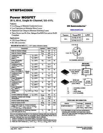
ntmfs4c06n.pdf 

NTMFS4C06N Power MOSFET 30 V, 69 A, Single N-Channel, SO-8 FL Features Low RDS(on) to Minimize Conduction Losses Low Capacitance to Minimize Driver Losses www.onsemi.com Optimized Gate Charge to Minimize Switching Losses These Devices are Pb-Free, Halogen Free/BFR Free and are RoHS V(BR)DSS RDS(ON) MAX ID MAX Compliant 4.0 mW @ 10 V Applications 30 V 69 A CPU P
6.14. Size:113K onsemi
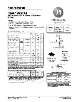
ntmfs4c01n.pdf 

NTMFS4C01N Power MOSFET 30 V, 0.9 mW, 303 A, Single N-Channel, SO-8FL Features Small Footprint (5x6 mm) for Compact Design http //onsemi.com Low RDS(on) to Minimize Conduction Losses Low QG and Capacitance to Minimize Driver Losses V(BR)DSS RDS(ON) MAX ID MAX These Devices are Pb-Free, Halogen Free/BFR Free and are RoHS Compliant 0.9 mW @ 10 V 30 V 303 A 1.2 mW @
6.15. Size:182K onsemi
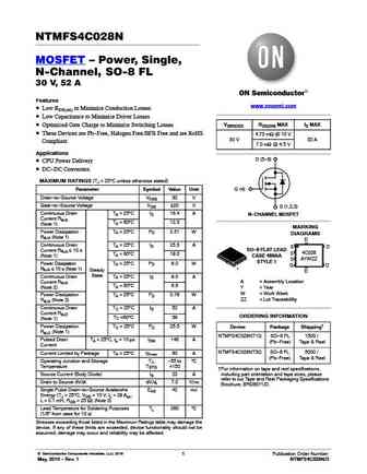
ntmfs4c028n.pdf 

NTMFS4C028N MOSFET Power, Single, N-Channel, SO-8 FL 30 V, 52 A Features www.onsemi.com Low RDS(on) to Minimize Conduction Losses Low Capacitance to Minimize Driver Losses V(BR)DSS RDS(ON) MAX ID MAX Optimized Gate Charge to Minimize Switching Losses These Devices are Pb-Free, Halogen Free/BFR Free and are RoHS 4.73 mW @ 10 V 30 V 52 A Compliant 7.0 mW @ 4.5 V
6.16. Size:173K onsemi
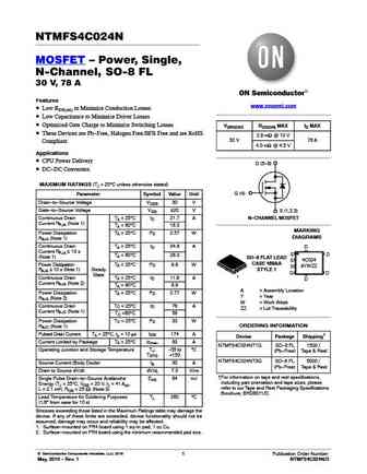
ntmfs4c024n.pdf 

NTMFS4C024N MOSFET Power, Single, N-Channel, SO-8 FL 30 V, 78 A Features www.onsemi.com Low RDS(on) to Minimize Conduction Losses Low Capacitance to Minimize Driver Losses Optimized Gate Charge to Minimize Switching Losses V(BR)DSS RDS(ON) MAX ID MAX These Devices are Pb-Free, Halogen Free/BFR Free and are RoHS 2.8 mW @ 10 V 30 V 78 A Compliant 4.0 mW @ 4.5 V
Otros transistores... NTMFS4982NF, NTMFS4983NF, NTMFS4985NF, NTMFS4C01N, NTMFS4C03N, NTMFS4C05N, NTMFS4C06N, NTMFS4C08N, IRFB4115, NTMFS4C10N, NTMFS4C13N, NTMFS4C35N, NTMFS4H01N, NTMFS4H01NF, NTMFS4H02N, NTMFS4H02NF, NTMFS5830NLT1G

