NTTFS3A08PZTAG Datasheet. Equivalente. Reemplazo. Hoja de especificaciones. Principales características
Número de Parte: NTTFS3A08PZTAG 📄📄
Tipo de FET: MOSFET
Polaridad de transistor: P
ESPECIFICACIONES MÁXIMAS
Pdⓘ - Máxima disipación de potencia: 0.84 W
|Vds|ⓘ - Voltaje máximo drenador-fuente: 20 V
|Vgs|ⓘ - Voltaje máximo fuente-puerta: 8 V
|Id|ⓘ - Corriente continua de drenaje: 14 A
Tjⓘ - Temperatura máxima de unión: 150 °C
CARACTERÍSTICAS ELÉCTRICAS
trⓘ - Tiempo de subida: 60 nS
Cossⓘ - Capacitancia de salida: 600 pF
RDSonⓘ - Resistencia estado encendido drenaje a fuente: 0.0067 Ohm
Encapsulados: WDFN8
📄📄 Copiar
Búsqueda de reemplazo de NTTFS3A08PZTAG MOSFET
- Selecciónⓘ de transistores por parámetros
NTTFS3A08PZTAG datasheet
nttfs3a08pz nttfs3a08pztag.pdf
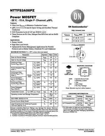
NTTFS3A08PZ Power MOSFET -20 V, -15 A, Single P-Channel, m8FL Features Ultra Low RDS(on) to Minimize Conduction Losses m8FL 3.3 x 3.3 x 0.8 mm for Space Saving and Excellent Thermal Conduction http //onsemi.com ESD Protection Level of 5 kV per JESD22-A114 These Devices are Pb-Free, Halogen Free/BFR Free and are RoHS V(BR)DSS RDS(on) MAX ID MAX Compliant 6.7 mW @ -4.5
nttfs5820nltag.pdf

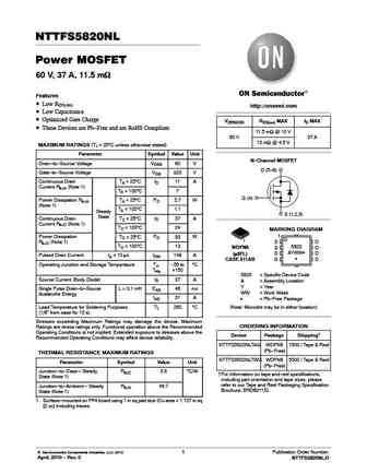
NTTFS5820NL Power MOSFET 60 V, 37 A, 11.5 mW Features Low RDS(on) http //onsemi.com Low Capacitance Optimized Gate Charge V(BR)DSS RDS(on) MAX ID MAX These Devices are Pb-Free and are RoHS Compliant 11.5 mW @ 10 V 60 V 37 A 15 mW @ 4.5 V MAXIMUM RATINGS (TJ = 25 C unless otherwise stated) Parameter Symbol Value Unit N-Channel MOSFET Drain-to-Source Voltage VDSS
nttfs4c25ntag.pdf

NTTFS4C25N Power MOSFET 30 V, 27 A, Single N-Channel, m8FL Features Low RDS(on) to Minimize Conduction Losses Low Capacitance to Minimize Driver Losses Optimized Gate Charge to Minimize Switching Losses http //onsemi.com These Devices are Pb-Free, Halogen Free/BFR Free and are RoHS Compliant V(BR)DSS RDS(on) MAX ID MAX Applications 17 mW @ 10 V DC-DC Converters
nttfs4928ntag.pdf
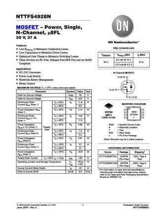
NTTFS4928N MOSFET Power, Single, N-Channel, m8FL 30 V, 37 A Features http //onsemi.com Low RDS(on) to Minimize Conduction Losses Low Capacitance to Minimize Driver Losses V(BR)DSS RDS(on) MAX ID MAX Optimized Gate Charge to Minimize Switching Losses 9.0 mW @ 10 V These Devices are Pb-Free, Halogen Free/BFR Free and are RoHS 30 V 37 A Compliant 13.5 mW @ 4.5 V
nttfs4c10ntag.pdf
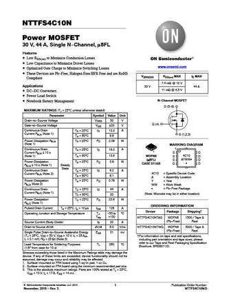
NTTFS4C10N Power MOSFET 30 V, 44 A, Single N-Channel, m8FL Features Low RDS(on) to Minimize Conduction Losses Low Capacitance to Minimize Driver Losses www.onsemi.com Optimized Gate Charge to Minimize Switching Losses These Devices are Pb-Free, Halogen Free/BFR Free and are RoHS V(BR)DSS RDS(on) MAX ID MAX Compliant 7.4 mW @ 10 V Applications 30 V 44 A 11 mW @ 4.5
nttfs5116pltag.pdf

NTTFS5116PL MOSFET Power -60 V, -20 A, 52 mW Features Low RDS(on) Fast Switching www.onsemi.com These Devices are Pb-Free and are RoHS Compliant V(BR)DSS RDS(on) MAX ID MAX Applications 52 mW @ -10 V Load Switches -60 V -20 A DC Motor Control 72 mW @ -4.5 V DC-DC Conversion P-Channel MOSFET MAXIMUM RATINGS (TJ = 25 C unless otherwise stated) D (5-8
nttfs5c454nltag.pdf
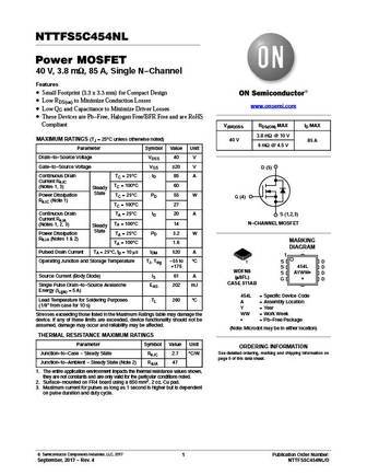
NTTFS5C454NL Power MOSFET 40 V, 3.8 mW, 85 A, Single N-Channel Features Small Footprint (3.3 x 3.3 mm) for Compact Design Low RDS(on) to Minimize Conduction Losses www.onsemi.com Low QG and Capacitance to Minimize Driver Losses These Devices are Pb-Free, Halogen Free/BFR Free and are RoHS Compliant V(BR)DSS RDS(ON) MAX ID MAX 3.8 mW @ 10 V MAXIMUM RATINGS (TJ = 25 C
nttfs5826nltag.pdf

NTTFS5826NL Power MOSFET 60 V, 24 mW, Single N-Channel, m8FL Features Small Footprint (3.3 x 3.3 mm) for Compact Designs Low QG(TOT) to Minimize Switching Losses Low Capacitance to Minimize Driver Losses http //onsemi.com These are Pb-Free Devices V(BR)DSS RDS(on) MAX ID MAX Applications Motor Drivers 24 mW @ 10 V 60 V 20 A DC-DC Converters 32 mW @ 4.5 V
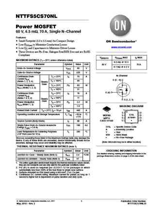
nttfs5c670nl.pdf

NTTFS5C670NL Power MOSFET 60 V, 6.5 mW, 70 A, Single N-Channel Features Small Footprint (3.3 x 3.3 mm) for Compact Design Low RDS(on) to Minimize Conduction Losses www.onsemi.com Low QG and Capacitance to Minimize Driver Losses These Devices are Pb-Free, Halogen Free/BFR Free and are RoHS Compliant V(BR)DSS RDS(on) MAX ID MAX MAXIMUM RATINGS (TJ = 25 C unless otherwi
nttfs4932n.pdf

NTTFS4932N MOSFET Power, Single, N-Channel, m8FL 30 V, 79 A Features http //onsemi.com Low RDS(on) to Minimize Conduction Losses Low Capacitance to Minimize Driver Losses V(BR)DSS RDS(on) MAX ID MAX Optimized Gate Charge to Minimize Switching Losses These Devices are Pb-Free, Halogen Free/BFR Free and are RoHS 4.0 mW @ 10 V 30 V 79 A Compliant 5.5 mW @ 4.5 V A
nttfs004n04c.pdf

NTTFS004N04C MOSFET Power, Single, N-Channel 40 V, 4.9 mW, 77 A Features www.onsemi.com Small Footprint (3.3 x 3.3 mm) for Compact Design Low RDS(on) to Minimize Conduction Losses Low Capacitance to Minimize Driver Losses These Devices are Pb-Free and are RoHS Compliant V(BR)DSS RDS(on) MAX ID MAX 40 V 4.9 mW @ 10 V 77 A MAXIMUM RATINGS (TJ = 25 C unless otherwis
nttfs5d1n06hl.pdf
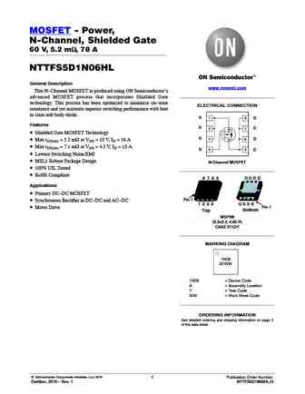
MOSFET - Power, N-Channel, Shielded Gate 60 V, 5.2 mW, 78 A NTTFS5D1N06HL General Description www.onsemi.com This N-Channel MOSFET is produced using ON Semiconductor s advanced MOSFET process that incorporates Shielded Gate technology. This process has been optimized to minimize on-state ELECTRICAL CONNECTION resistance and yet maintain superior switching performance with best in c
nttfs4932ntag.pdf

NTTFS4932N Power MOSFET 30 V, 79 A, Single N-Channel, m8FL Features Low RDS(on) to Minimize Conduction Losses Low Capacitance to Minimize Driver Losses http //onsemi.com Optimized Gate Charge to Minimize Switching Losses These Devices are Pb-Free, Halogen Free/BFR Free and are RoHS V(BR)DSS RDS(on) MAX ID MAX Compliant Applications 4.0 mW @ 10 V 30 V 79 A Low-S
nttfs4823ntag.pdf

NTTFS4823N Power MOSFET 30 V, 50 A, Single N-Channel, m8FL Features Small Footprint (3.3 x 3.3 mm) for Compact Design Low RDS(on) to Minimize Conduction Losses http //onsemi.com Low Capacitance to Minimize Driver Losses These Devices are Pb-Free, Halogen Free/BFR Free and are RoHS V(BR)DSS RDS(on) MAX ID MAX Compliant 10.5 mW @ 10 V 30 V 50 A Applications 17.5 mW @
nttfs4929ntag.pdf

NTTFS4929N Power MOSFET 30 V, 34 A, Single N-Channel, m8FL Features Low RDS(on) to Minimize Conduction Losses Low Capacitance to Minimize Driver Losses http //onsemi.com Optimized Gate Charge to Minimize Switching Losses These Devices are Pb-Free, Halogen Free/BFR Free and are RoHS V(BR)DSS RDS(on) MAX ID MAX Compliant 11 mW @ 10 V Applications 30 V 34 A 17 mW @ 4.
nttfs5820nltag.pdf
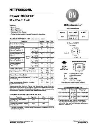
NTTFS5820NL Power MOSFET 60 V, 37 A, 11.5 mW Features Low RDS(on) http //onsemi.com Low Capacitance Optimized Gate Charge V(BR)DSS RDS(on) MAX ID MAX These Devices are Pb-Free and are RoHS Compliant 11.5 mW @ 10 V 60 V 37 A 15 mW @ 4.5 V MAXIMUM RATINGS (TJ = 25 C unless otherwise stated) Parameter Symbol Value Unit N-Channel MOSFET Drain-to-Source Voltage VDSS
nttfs8d1n08h.pdf
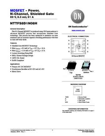
MOSFET - Power, N-Channel, Shielded Gate 80 V, 8.3 mW, 61 A NTTFS8D1N08H General Description www.onsemi.com This N-Channel MOSFET is produced using ON Semiconductor s advanced MOSFET process that incorporates Shielded Gate technology. This process has been optimized to minimize on-state ELECTRICAL CONNECTION resistance and yet maintain superior switching performance with best in cl
nttfs4930n.pdf

NTTFS4930N Power MOSFET 30 V, 23 A, Single N-Channel, m8FL Features Low RDS(on) to Minimize Conduction Losses Low Capacitance to Minimize Driver Losses http //onsemi.com Optimized Gate Charge to Minimize Switching Losses These Devices are Pb-Free, Halogen Free/BFR Free and are RoHS V(BR)DSS RDS(on) MAX ID MAX Compliant Applications 23 mW @ 10 V 30 V 23 A DC-DC
nttfs4939n-d.pdf

NTTFS4939N Power MOSFET 30 V, 52 A, Single N-Channel, m8FL Features Low RDS(on) to Minimize Conduction Losses Low Capacitance to Minimize Driver Losses http //onsemi.com Optimized Gate Charge to Minimize Switching Losses These Devices are Pb-Free, Halogen Free/BFR Free and are RoHS V(BR)DSS RDS(on) MAX ID MAX Compliant Applications 5.5 mW @ 10 V 30 V 52 A Low-S
nttfs5c658nl.pdf
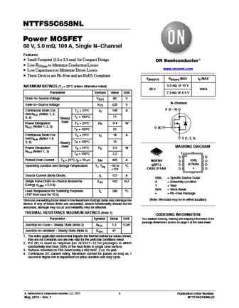
NTTFS5C658NL Power MOSFET 60 V, 5.0 mW, 109 A, Single N-Channel Features Small Footprint (3.3 x 3.3 mm) for Compact Design Low RDS(on) to Minimize Conduction Losses www.onsemi.com Low Capacitance to Minimize Driver Losses These Devices are Pb-Free and are RoHS Compliant V(BR)DSS RDS(on) MAX ID MAX 5.0 mW @ 10 V MAXIMUM RATINGS (TJ = 25 C unless otherwise noted) 60 V
nttfs4941n.pdf

NTTFS4941N Power MOSFET 30 V, 46 A, Single N-Channel, m8FL Features Low RDS(on) to Minimize Conduction Losses Low Capacitance to Minimize Driver Losses http //onsemi.com Optimized Gate Charge to Minimize Switching Losses These Devices are Pb-Free, Halogen Free/BFR Free and are RoHS V(BR)DSS RDS(on) MAX ID MAX Compliant Applications 6.2 mW @ 10 V 30 V 46 A Low-S
nttfs4c06n.pdf

NTTFS4C06N Power MOSFET 30 V, 67 A, Single N-Channel, m8FL Features Low RDS(on) to Minimize Conduction Losses Low Capacitance to Minimize Driver Losses http //onsemi.com Optimized Gate Charge to Minimize Switching Losses These Devices are Pb-Free, Halogen Free/BFR Free and are RoHS V(BR)DSS RDS(on) MAX ID MAX Compliant 4.2 mW @ 10 V Applications 30 V 67 A 6.1 mW @
nttfs5826nl.pdf

NTTFS5826NL Power MOSFET 60 V, 24 mW, Single N-Channel, m8FL Features Small Footprint (3.3 x 3.3 mm) for Compact Designs Low QG(TOT) to Minimize Switching Losses Low Capacitance to Minimize Driver Losses http //onsemi.com These are Pb-Free Devices V(BR)DSS RDS(on) MAX ID MAX Applications Motor Drivers 24 mW @ 10 V 60 V 20 A DC-DC Converters 32 mW @ 4.5 V
nttfs015p03p8z.pdf
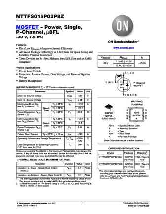
NTTFS015P03P8Z MOSFET Power, Single, P-Channel, m8FL -30 V, 7.5 mW Features www.onsemi.com Ultra Low RDS(on) to Improve System Efficiency Advanced Package Technology in 3.3x3.3mm for Space Saving and Excellent Thermal Conduction V(BR)DSS RDS(on) ID These Devices are Pb-Free, Halogen Free/BFR Free and are RoHS 7.5 mW @ -10 V Compliant -30 V -47.6 A 12 mW @ -4.5 V
nttfs2d8n04hl.pdf

MOSFET - Power, N-Channel, Shielded Gate 40 V, 2.75 mW, 104 A NTTFS2D8N04HL General Description www.onsemi.com This N-Channel MOSFET is produced using ON Semiconductor s advanced MOSFET process that incorporates Shielded Gate technology. This process has been optimized to minimize on-state ELECTRICAL CONNECTION resistance and yet maintain superior switching performance with best in
nttfs4928n.pdf
NTTFS4928N Power MOSFET 30 V, 37 A, Single N-Channel, m8FL Features Low RDS(on) to Minimize Conduction Losses Low Capacitance to Minimize Driver Losses http //onsemi.com Optimized Gate Charge to Minimize Switching Losses These Devices are Pb-Free, Halogen Free/BFR Free and are RoHS V(BR)DSS RDS(on) MAX ID MAX Compliant 9.0 mW @ 10 V Applications 30 V 37 A 13.5 mW @
nttfs4824n.pdf
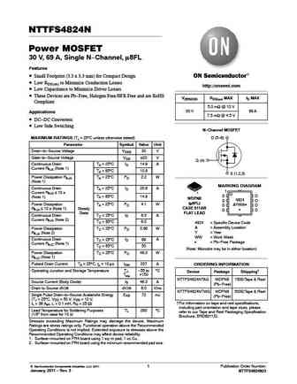
NTTFS4824N Power MOSFET 30 V, 69 A, Single N-Channel, m8FL Features Small Footprint (3.3 x 3.3 mm) for Compact Design Low RDS(on) to Minimize Conduction Losses http //onsemi.com Low Capacitance to Minimize Driver Losses These Devices are Pb-Free, Halogen Free/BFR Free and are RoHS V(BR)DSS RDS(on) MAX ID MAX Compliant 5.0 mW @ 10 V 30 V 69 A Applications 7.5 mW @ 4
nttfs005n04c.pdf
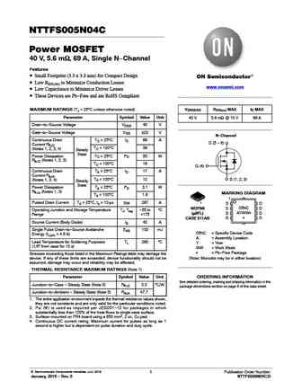
NTTFS005N04C Power MOSFET 40 V, 5.6 mW, 69 A, Single N-Channel Features Small Footprint (3.3 x 3.3 mm) for Compact Design Low RDS(on) to Minimize Conduction Losses www.onsemi.com Low Capacitance to Minimize Driver Losses These Devices are Pb-Free and are RoHS Compliant V(BR)DSS RDS(on) MAX ID MAX MAXIMUM RATINGS (TJ = 25 C unless otherwise noted) Parameter Symbol Val
nttfs5c478nl.pdf

MOSFET Power, Single N-Channel 40 V, 14 mW, 26 A NTTFS5C478NL Features Small Footprint (3.3 x 3.3 mm) for Compact Design www.onsemi.com Low RDS(on) to Minimize Conduction Losses Low Capacitance to Minimize Driver Losses These Devices are Pb-Free and are RoHS Compliant V(BR)DSS RDS(on) MAX ID MAX 14 mW @ 10 V MAXIMUM RATINGS (TJ = 25 C unless otherwise noted) 40
nttfs016n06c.pdf
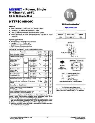
MOSFET - Power, Single N-Channel, m8FL 60 V, 16.3 mW, 32 A NTTFS016N06C Features www.onsemi.com Small Footprint (3.3 x 3.3 mm) for Compact Design Low RDS(on) to Minimize Conduction Losses Low QG and Capacitance to Minimize Driver Losses V(BR)DSS RDS(on) MAX ID MAX These Devices are Pb-Free, Halogen Free/BFR Free and are RoHS Compliant 60 V 16.3 mW @ 10 V 32 A Typica
nttfs5c454nl.pdf
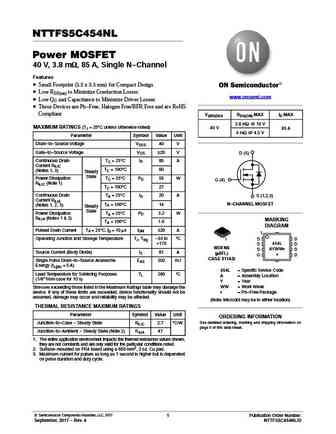
NTTFS5C454NL Power MOSFET 40 V, 3.8 mW, 85 A, Single N-Channel Features Small Footprint (3.3 x 3.3 mm) for Compact Design Low RDS(on) to Minimize Conduction Losses www.onsemi.com Low QG and Capacitance to Minimize Driver Losses These Devices are Pb-Free, Halogen Free/BFR Free and are RoHS Compliant V(BR)DSS RDS(ON) MAX ID MAX 3.8 mW @ 10 V MAXIMUM RATINGS (TJ = 25 C
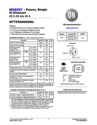
nttfs6h850n.pdf
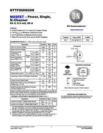
NTTFS6H850N MOSFET Power, Single, N-Channel 80 V, 9.5 mW, 68 A Features www.onsemi.com Small Footprint (3.3 x 3.3 mm) for Compact Design Low RDS(on) to Minimize Conduction Losses Low Capacitance to Minimize Driver Losses These Devices are Pb-Free and are RoHS Compliant V(BR)DSS RDS(on) MAX ID MAX 80 V 9.5 mW @ 10 V 68 A MAXIMUM RATINGS (TJ = 25 C unless otherwise
nttfs4h05n nttfs4h05ntag.pdf
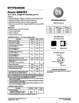
NTTFS4H05N Power MOSFET 25 V, 94 A, Single N-Channel, m8-FL Features Optimized Design to Minimize Conduction and Switching Losses Optimized Package to Minimize Parasitic Inductances Optimized material for improved thermal performance http //onsemi.com These Devices are Pb-Free, Halogen Free/BFR Free and are RoHS Compliant Applications VGS MAX RDS(on) TYP QGTOT Hi
nttfs4941ntag.pdf

NTTFS4941N Power MOSFET 30 V, 46 A, Single N-Channel, m8FL Features Low RDS(on) to Minimize Conduction Losses Low Capacitance to Minimize Driver Losses http //onsemi.com Optimized Gate Charge to Minimize Switching Losses These Devices are Pb-Free, Halogen Free/BFR Free and are RoHS V(BR)DSS RDS(on) MAX ID MAX Compliant Applications 6.2 mW @ 10 V 30 V 46 A Low-S
nttfs4937n.pdf

NTTFS4937N MOSFET Power, Single, N-Channel, m8FL 30 V, 75 A Features http //onsemi.com Low RDS(on) to Minimize Conduction Losses Low Capacitance to Minimize Driver Losses V(BR)DSS RDS(on) MAX ID MAX Optimized Gate Charge to Minimize Switching Losses These Devices are Pb-Free, Halogen Free/BFR Free and are RoHS 4.5 mW @ 10 V 30 V 75 A Compliant 7.0 mW @ 4.5 V A
nttfs4c02n.pdf
NTTFS4C02N MOSFET Power, Single, N-Channel, m8FL 30 V, 170 A Features Low RDS(on) to Minimize Conduction Losses www.onsemi.com Low Capacitance to Minimize Driver Losses Optimized Gate Charge to Minimize Switching Losses V(BR)DSS RDS(on) MAX ID MAX These Devices are Pb-Free, Halogen Free/BFR Free and are RoHS Compliant 2.25 mW @ 10 V 30 V 170 A Applications 3.1
nttfs4939n.pdf
NTTFS4939N MOSFET Power, Single, N-Channel, m8FL 30 V, 52 A Features http //onsemi.com Low RDS(on) to Minimize Conduction Losses Low Capacitance to Minimize Driver Losses V(BR)DSS RDS(on) MAX ID MAX Optimized Gate Charge to Minimize Switching Losses These Devices are Pb-Free, Halogen Free/BFR Free and are RoHS 5.5 mW @ 10 V 30 V 52 A Compliant 8.0 mW @ 4.5 V A
nttfs4928ntag.pdf

NTTFS4928N Power MOSFET 30 V, 37 A, Single N-Channel, m8FL Features Low RDS(on) to Minimize Conduction Losses Low Capacitance to Minimize Driver Losses http //onsemi.com Optimized Gate Charge to Minimize Switching Losses These Devices are Pb-Free, Halogen Free/BFR Free and are RoHS V(BR)DSS RDS(on) MAX ID MAX Compliant 9.0 mW @ 10 V Applications 30 V 37 A 13.5 mW @
nttfs030n06c.pdf
MOSFET - Power, Single N-Channel, m8FL 60 V, 29.7 mW, 19 A NTTFS030N06C Features www.onsemi.com Small Footprint (3.3 x 3.3 mm) for Compact Design Low RDS(on) to Minimize Conduction Losses Low QG and Capacitance to Minimize Driver Losses V(BR)DSS RDS(on) MAX ID MAX These Devices are Pb-Free, Halogen Free/BFR Free and are RoHS Compliant 60 V 29.7 mW @ 10 V 19 A Typica
nttfs4824ntag.pdf

NTTFS4824N Power MOSFET 30 V, 69 A, Single N-Channel, m8FL Features Small Footprint (3.3 x 3.3 mm) for Compact Design Low RDS(on) to Minimize Conduction Losses http //onsemi.com Low Capacitance to Minimize Driver Losses These Devices are Pb-Free, Halogen Free/BFR Free and are RoHS V(BR)DSS RDS(on) MAX ID MAX Compliant 5.0 mW @ 10 V 30 V 69 A Applications 7.5 mW @ 4
nttfs6h860nl.pdf

MOSFET - Power, Single N-Channel 80 V, 20 mW, 30 A NTTFS6H860NL Features Small Footprint (3.3 x 3.3 mm) for Compact Design www.onsemi.com Low RDS(on) to Minimize Conduction Losses Low Capacitance to Minimize Driver Losses V(BR)DSS RDS(ON) MAX ID MAX These Devices are Pb-Free and are RoHS Compliant 20 mW @ 10 V MAXIMUM RATINGS (TJ = 25 C unless otherwise noted) 80 V
nttfs4939ntag.pdf

NTTFS4939N Power MOSFET 30 V, 52 A, Single N-Channel, m8FL Features Low RDS(on) to Minimize Conduction Losses Low Capacitance to Minimize Driver Losses http //onsemi.com Optimized Gate Charge to Minimize Switching Losses These Devices are Pb-Free, Halogen Free/BFR Free and are RoHS V(BR)DSS RDS(on) MAX ID MAX Compliant Applications 5.5 mW @ 10 V 30 V 52 A Low-S
nttfs5116pl-d.pdf

NTTFS5116PL Power MOSFET -60 V, -20 A, 52 mW Features Low RDS(on) Fast Switching http //onsemi.com These Devices are Pb-Free and are RoHS Compliant Applications V(BR)DSS RDS(on) MAX ID MAX Load Switches 52 mW @ -10 V DC Motor Control -60 V -20 A 72 mW @ -4.5 V DC-DC Conversion MAXIMUM RATINGS (TJ = 25 C unless otherwise stated) P-Channel MOSFET Parameter
nttfs008n04c.pdf
NTTFS008N04C Power MOSFET 40 V, 7.1 mW, 48 A, Single N-Channel Features Small Footprint (3.3 x 3.3 mm) for Compact Design Low RDS(on) to Minimize Conduction Losses www.onsemi.com Low Capacitance to Minimize Driver Losses These Devices are Pb-Free and are RoHS Compliant MAXIMUM RATINGS (TJ = 25 C unless otherwise noted) V(BR)DSS RDS(on) MAX ID MAX Parameter Symbol Val
nttfs4943n-d.pdf

NTTFS4943N Power MOSFET 30 V, 41 A, Single N-Channel, m8FL Features Low RDS(on) to Minimize Conduction Losses Low Capacitance to Minimize Driver Losses http //onsemi.com Optimized Gate Charge to Minimize Switching Losses These Devices are Pb-Free, Halogen Free/BFR Free and are RoHS V(BR)DSS RDS(on) MAX ID MAX Compliant Applications 7.2 mW @ 10 V 30 V 41 A DC-DC
nttfs5811nl.pdf
NTTFS5811NL Power MOSFET 40 V, 53 A, 6.4 mW Features Low RDS(on) http //onsemi.com Low Capacitance Optimized Gate Charge V(BR)DSS RDS(on) MAX ID MAX These Devices are Pb-Free and are RoHS Compliant 6.7 mW @ 10 V 40 V 53 A 10 mW @ 4.5 V MAXIMUM RATINGS (TJ = 25 C unless otherwise stated) Parameter Symbol Value Unit N-Channel MOSFET Drain-to-Source Voltage VDSS 40
nttfs4c25n.pdf

NTTFS4C25N Power MOSFET 30 V, 27 A, Single N-Channel, m8FL Features Low RDS(on) to Minimize Conduction Losses Low Capacitance to Minimize Driver Losses Optimized Gate Charge to Minimize Switching Losses http //onsemi.com These Devices are Pb-Free, Halogen Free/BFR Free and are RoHS Compliant V(BR)DSS RDS(on) MAX ID MAX Applications 17 mW @ 10 V DC-DC Converters
nttfs4929n.pdf

NTTFS4929N Power MOSFET 30 V, 34 A, Single N-Channel, m8FL Features Low RDS(on) to Minimize Conduction Losses Low Capacitance to Minimize Driver Losses http //onsemi.com Optimized Gate Charge to Minimize Switching Losses These Devices are Pb-Free, Halogen Free/BFR Free and are RoHS V(BR)DSS RDS(on) MAX ID MAX Compliant 11 mW @ 10 V Applications 30 V 34 A 17 mW @ 4.
nttfs5cs70nl.pdf
NTTFS5CS70NL Power MOSFET 60 V, 6.5 mW, 70 A, Single N-Channel Features Small Footprint (3.3 x 3.3 mm) for Compact Design Low RDS(on) to Minimize Conduction Losses www.onsemi.com Low QG and Capacitance to Minimize Driver Losses These Devices are Pb-Free, Halogen Free/BFR Free and are RoHS Compliant V(BR)DSS RDS(on) MAX ID MAX MAXIMUM RATINGS (TJ = 25 C unless otherwi
nttfs003n04c.pdf

NTTFS003N04C MOSFET Power, Single, N-Channel 40 V, 3.5 mW, 103 A Features www.onsemi.com Small Footprint (3.3 x 3.3 mm) for Compact Design Low RDS(on) to Minimize Conduction Losses Low Capacitance to Minimize Driver Losses These Devices are Pb-Free and are RoHS Compliant V(BR)DSS RDS(on) MAX ID MAX 40 V 3.5 mW @ 10 V 103 A MAXIMUM RATINGS (TJ = 25 C unless otherw
nttfs015n04c.pdf

NTTFS015N04C MOSFET Power, Single, N-Channel 40 V, 17.3 mW, 27 A Features www.onsemi.com Small Footprint (3.3 x 3.3 mm) for Compact Design Low RDS(on) to Minimize Conduction Losses Low Capacitance to Minimize Driver Losses These Devices are Pb-Free and are RoHS Compliant V(BR)DSS RDS(on) MAX ID MAX 40 V 17.3 mW @ 10 V 27 A MAXIMUM RATINGS (TJ = 25 C unless otherw
nttfs5c680nl.pdf
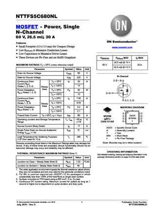
NTTFS5C680NL MOSFET - Power, Single N-Channel 60 V, 26.5 mW, 20 A Features Small Footprint (3.3 x 3.3 mm) for Compact Design www.onsemi.com Low RDS(on) to Minimize Conduction Losses Low Capacitance to Minimize Driver Losses These Devices are Pb-Free and are RoHS Compliant V(BR)DSS RDS(on) MAX ID MAX 26.5 mW @ 10 V MAXIMUM RATINGS (TJ = 25 C unless otherwise noted) 6
nttfs4h07n.pdf
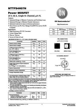
NTTFS4H07N Power MOSFET 25 V, 66 A, Single N-Channel, m8-FL Features Optimized Design to Minimize Conduction and Switching Losses Optimized Package to Minimize Parasitic Inductances Optimized material for improved thermal performance http //onsemi.com These Devices are Pb-Free, Halogen Free/BFR Free and are RoHS Compliant VGS MAX RDS(on) TYP QGTOT Applications Hi
nttfs5c673nl.pdf
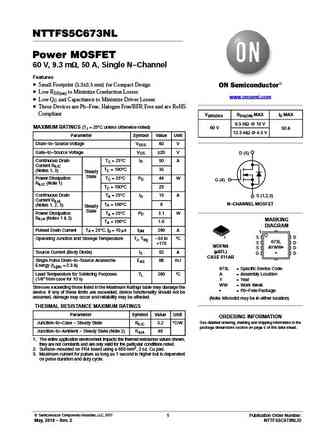
NTTFS5C673NL Power MOSFET 60 V, 9.3 mW, 50 A, Single N-Channel Features Small Footprint (3.3x3.3 mm) for Compact Design Low RDS(on) to Minimize Conduction Losses www.onsemi.com Low QG and Capacitance to Minimize Driver Losses These Devices are Pb-Free, Halogen Free/BFR Free and are RoHS Compliant V(BR)DSS RDS(ON) MAX ID MAX 9.3 mW @ 10 V MAXIMUM RATINGS (TJ = 25 C u
nttfs5820nl.pdf
NTTFS5820NL Power MOSFET 60 V, 37 A, 11.5 mW Features Low RDS(on) http //onsemi.com Low Capacitance Optimized Gate Charge V(BR)DSS RDS(on) MAX ID MAX These Devices are Pb-Free and are RoHS Compliant 11.5 mW @ 10 V 60 V 37 A 15 mW @ 4.5 V MAXIMUM RATINGS (TJ = 25 C unless otherwise stated) Parameter Symbol Value Unit N-Channel MOSFET Drain-to-Source Voltage VDSS
nttfs5826nl-d.pdf
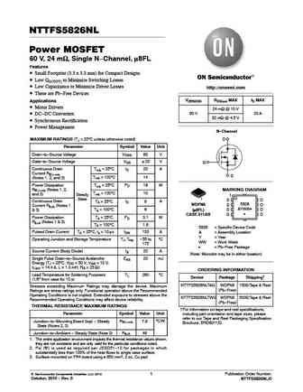
NTTFS5826NL Power MOSFET 60 V, 24 mW, Single N-Channel, m8FL Features Small Footprint (3.3 x 3.3 mm) for Compact Designs Low QG(TOT) to Minimize Switching Losses Low Capacitance to Minimize Driver Losses http //onsemi.com These are Pb-Free Devices V(BR)DSS RDS(on) MAX ID MAX Applications Motor Drivers 24 mW @ 10 V 60 V 20 A DC-DC Converters 32 mW @ 4.5 V
nttfs5c466nl.pdf
MOSFET Power, Single, N-Channel 40 V, 7.3 mW, 51 A NTTFS5C466NL Features www.onsemi.com Small Footprint (3.3 x 3.3 mm) for Compact Design Low RDS(on) to Minimize Conduction Losses Low Capacitance to Minimize Driver Losses V(BR)DSS RDS(on) MAX ID MAX These Devices are Pb-Free and are RoHS Compliant 7.3 mW @ 10 V 40 V 51 A MAXIMUM RATINGS (TJ = 25 C unless otherw
nttfs4930ntag.pdf

NTTFS4930N Power MOSFET 30 V, 23 A, Single N-Channel, m8FL Features Low RDS(on) to Minimize Conduction Losses Low Capacitance to Minimize Driver Losses http //onsemi.com Optimized Gate Charge to Minimize Switching Losses These Devices are Pb-Free, Halogen Free/BFR Free and are RoHS V(BR)DSS RDS(on) MAX ID MAX Compliant Applications 23 mW @ 10 V 30 V 23 A DC-DC
nttfs4945n.pdf

NTTFS4945N Power MOSFET 30 V, 34 A, Single N-Channel, m8FL Features Low RDS(on) to Minimize Conduction Losses Low Capacitance to Minimize Driver Losses http //onsemi.com Optimized Gate Charge to Minimize Switching Losses These Devices are Pb-Free, Halogen Free/BFR Free and are RoHS V(BR)DSS RDS(on) MAX ID MAX Compliant 9.0 mW @ 10 V Applications 30 V 34 A Power
nttfs5c460nl.pdf

NTTFS5C460NL MOSFET Power, Single, N-Channel 40 V, 4.8 mW, 74 A Features www.onsemi.com Small Footprint (3.3 x 3.3 mm) for Compact Design Low RDS(on) to Minimize Conduction Losses Low Capacitance to Minimize Driver Losses V(BR)DSS RDS(on) MAX ID MAX These Devices are Pb-Free and are RoHS Compliant 4.8 mW @ 10 V 40 V 74 A MAXIMUM RATINGS (TJ = 25 C unless otherw
nttfs4c13n.pdf
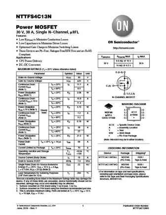
NTTFS4C13N Power MOSFET 30 V, 38 A, Single N-Channel, m8FL Features Low RDS(on) to Minimize Conduction Losses Low Capacitance to Minimize Driver Losses Optimized Gate Charge to Minimize Switching Losses http //onsemi.com These Devices are Pb-Free, Halogen Free/BFR Free and are RoHS Compliant V(BR)DSS RDS(ON) MAX ID MAX Applications 9.4 mW @ 10 V CPU Power Delive
nttfs4840n.pdf
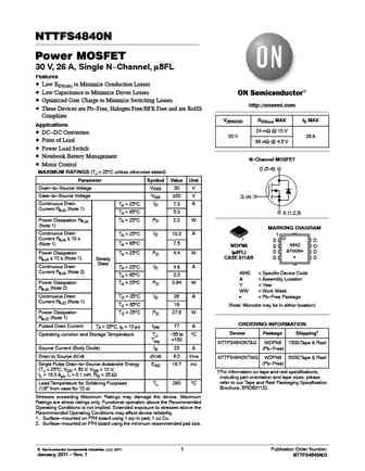
NTTFS4840N Power MOSFET 30 V, 26 A, Single N-Channel, m8FL Features Low RDS(on) to Minimize Conduction Losses Low Capacitance to Minimize Driver Losses Optimized Gate Charge to Minimize Switching Losses http //onsemi.com These Devices are Pb-Free, Halogen Free/BFR Free and are RoHS Compliant V(BR)DSS RDS(on) MAX ID MAX Applications 24 mW @ 10 V DC-DC Converters
nttfs4821ntag.pdf

NTTFS4821N Power MOSFET 30 V, 57 A, Single N-Channel, m8FL Features Small Footprint (3.3 x 3.3 mm) for Compact Design Low RDS(on) to Minimize Conduction Losses http //onsemi.com Low Capacitance to Minimize Driver Losses These Devices are Pb-Free, Halogen Free/BFR Free and are RoHS V(BR)DSS RDS(on) MAX ID MAX Compliant 7.0 mW @ 10 V 30 V 57 A Applications 10.8 mW @
nttfs4932n-d.pdf

NTTFS4932N Power MOSFET 30 V, 79 A, Single N-Channel, m8FL Features Low RDS(on) to Minimize Conduction Losses Low Capacitance to Minimize Driver Losses http //onsemi.com Optimized Gate Charge to Minimize Switching Losses These Devices are Pb-Free, Halogen Free/BFR Free and are RoHS V(BR)DSS RDS(on) MAX ID MAX Compliant Applications 4.0 mW @ 10 V 30 V 79 A Low-S
nttfs5811nltag.pdf

NTTFS5811NL Power MOSFET 40 V, 53 A, 6.4 mW Features Low RDS(on) http //onsemi.com Low Capacitance Optimized Gate Charge V(BR)DSS RDS(on) MAX ID MAX These Devices are Pb-Free and are RoHS Compliant 6.7 mW @ 10 V 40 V 53 A 10 mW @ 4.5 V MAXIMUM RATINGS (TJ = 25 C unless otherwise stated) Parameter Symbol Value Unit N-Channel MOSFET Drain-to-Source Voltage VDSS 40
nttfs024n06c.pdf
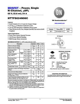
MOSFET - Power, Single N-Channel, m8FL 60 V, 22.6 mW, 24 A NTTFS024N06C Features www.onsemi.com Small Footprint (3.3 x 3.3 mm) for Compact Design Low RDS(on) to Minimize Conduction Losses Low QG and Capacitance to Minimize Driver Losses V(BR)DSS RDS(on) MAX ID MAX These Devices are Pb-Free, Halogen Free/BFR Free and are RoHS Compliant 60 V 22.6 mW @ 10 V 24 A Typica
nttfs4937n-d.pdf

NTTFS4937N Power MOSFET 30 V, 75 A, Single N-Channel, m8FL Features Low RDS(on) to Minimize Conduction Losses Low Capacitance to Minimize Driver Losses http //onsemi.com Optimized Gate Charge to Minimize Switching Losses These Devices are Pb-Free, Halogen Free/BFR Free and are RoHS V(BR)DSS RDS(on) MAX ID MAX Compliant Applications 4.5 mW @ 10 V 30 V 75 A Low-S
nttfs1d2n02p1e.pdf
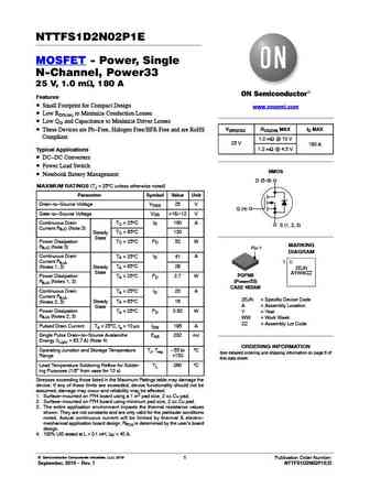
NTTFS1D2N02P1E MOSFET - Power, Single N-Channel, Power33 25 V, 1.0 mW, 180 A Features Small Footprint for Compact Design www.onsemi.com Low RDS(on) to Minimize Conduction Losses Low QG and Capacitance to Minimize Driver Losses V(BR)DSS RDS(ON) MAX ID MAX These Devices are Pb-Free, Halogen Free/BFR Free and are RoHS Compliant 1.0 mW @ 10 V 25 V 180 A 1.2 mW @ 4.5 V
nttfs5116pltag.pdf
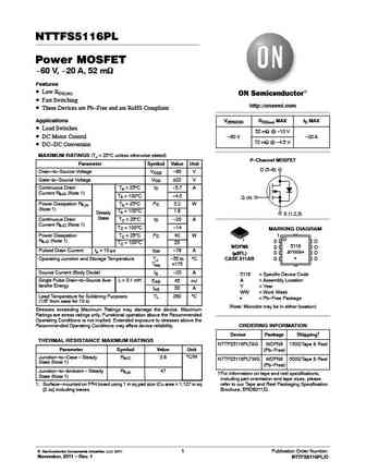
NTTFS5116PL Power MOSFET -60 V, -20 A, 52 mW Features Low RDS(on) Fast Switching http //onsemi.com These Devices are Pb-Free and are RoHS Compliant Applications V(BR)DSS RDS(on) MAX ID MAX Load Switches 52 mW @ -10 V DC Motor Control -60 V -20 A 72 mW @ -4.5 V DC-DC Conversion MAXIMUM RATINGS (TJ = 25 C unless otherwise stated) P-Channel MOSFET Parameter
nttfs4985nf.pdf
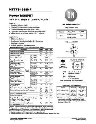
NTTFS4985NF Power MOSFET 30 V, 64 A, Single N-Channel, WDFN8 Features Integrated Schottky Diode Low RDS(on) to Minimize Conduction Losses http //onsemi.com Low Capacitance to Minimize Driver Losses Optimized Gate Charge to Minimize Switching Losses V(BR)DSS RDS(on) MAX ID MAX These Devices are Pb-Free and are RoHS Compliant 3.5 mW @ 10 V 30 V 64 A Applications
nttfs4821n.pdf

NTTFS4821N Power MOSFET 30 V, 57 A, Single N-Channel, m8FL Features Small Footprint (3.3 x 3.3 mm) for Compact Design Low RDS(on) to Minimize Conduction Losses http //onsemi.com Low Capacitance to Minimize Driver Losses These Devices are Pb-Free, Halogen Free/BFR Free and are RoHS V(BR)DSS RDS(on) MAX ID MAX Compliant 7.0 mW @ 10 V 30 V 57 A Applications 10.8 mW @
nttfs5116pl.pdf
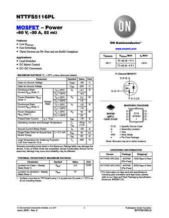
NTTFS5116PL MOSFET Power -60 V, -20 A, 52 mW Features Low RDS(on) Fast Switching www.onsemi.com These Devices are Pb-Free and are RoHS Compliant V(BR)DSS RDS(on) MAX ID MAX Applications 52 mW @ -10 V Load Switches -60 V -20 A DC Motor Control 72 mW @ -4.5 V DC-DC Conversion P-Channel MOSFET MAXIMUM RATINGS (TJ = 25 C unless otherwise stated) D (5-8
nttfs4823n.pdf

NTTFS4823N Power MOSFET 30 V, 50 A, Single N-Channel, m8FL Features Small Footprint (3.3 x 3.3 mm) for Compact Design Low RDS(on) to Minimize Conduction Losses http //onsemi.com Low Capacitance to Minimize Driver Losses These Devices are Pb-Free, Halogen Free/BFR Free and are RoHS V(BR)DSS RDS(on) MAX ID MAX Compliant 10.5 mW @ 10 V 30 V 50 A Applications 17.5 mW @
nttfs4c10n.pdf

NTTFS4C10N Power MOSFET 30 V, 44 A, Single N-Channel, m8FL Features Low RDS(on) to Minimize Conduction Losses Low Capacitance to Minimize Driver Losses Optimized Gate Charge to Minimize Switching Losses http //onsemi.com These Devices are Pb-Free, Halogen Free/BFR Free and are RoHS Compliant V(BR)DSS RDS(on) MAX ID MAX Applications 7.4 mW @ 10 V DC-DC Converters
nttfs4937ntag.pdf

NTTFS4937N Power MOSFET 30 V, 75 A, Single N-Channel, m8FL Features Low RDS(on) to Minimize Conduction Losses Low Capacitance to Minimize Driver Losses http //onsemi.com Optimized Gate Charge to Minimize Switching Losses These Devices are Pb-Free, Halogen Free/BFR Free and are RoHS V(BR)DSS RDS(on) MAX ID MAX Compliant Applications 4.5 mW @ 10 V 30 V 75 A Low-S
nttfs6h880nl.pdf
MOSFET - Power, Single N-Channel 80 V, 29 mW, 22 A NTTFS6H880NL Features Small Footprint (3.3 x 3.3 mm) for Compact Design www.onsemi.com Low RDS(on) to Minimize Conduction Losses Low Capacitance to Minimize Driver Losses V(BR)DSS RDS(ON) MAX ID MAX These Devices are Pb-Free and are RoHS Compliant 29 mW @ 10 V 80 V MAXIMUM RATINGS (TJ = 25 C unless otherwise noted)
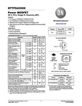
nttfs4c05n.pdf

NTTFS4C05N Power MOSFET 30 V, 75 A, Single N-Channel, m8FL Features Low RDS(on) to Minimize Conduction Losses Low Capacitance to Minimize Driver Losses Optimized Gate Charge to Minimize Switching Losses http //onsemi.com These Devices are Pb-Free, Halogen Free/BFR Free and are RoHS Compliant V(BR)DSS RDS(on) MAX ID MAX Applications 3.6 mW @ 10 V DC-DC Converters
nttfs5826nltag.pdf

NTTFS5826NL Power MOSFET 60 V, 24 mW, Single N-Channel, m8FL Features Small Footprint (3.3 x 3.3 mm) for Compact Designs Low QG(TOT) to Minimize Switching Losses Low Capacitance to Minimize Driver Losses http //onsemi.com These are Pb-Free Devices V(BR)DSS RDS(on) MAX ID MAX Applications Motor Drivers 24 mW @ 10 V 60 V 20 A DC-DC Converters 32 mW @ 4.5 V
nttfs002n04cl.pdf
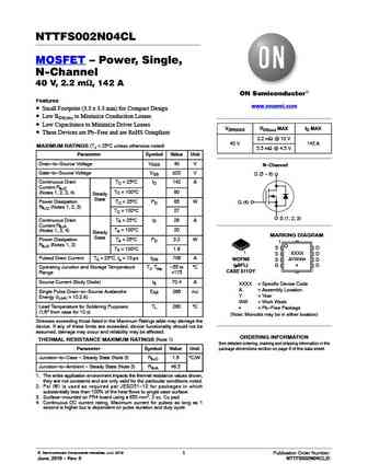
NTTFS002N04CL MOSFET Power, Single, N-Channel 40 V, 2.2 mW, 142 A Features www.onsemi.com Small Footprint (3.3 x 3.3 mm) for Compact Design Low RDS(on) to Minimize Conduction Losses Low Capacitance to Minimize Driver Losses V(BR)DSS RDS(on) MAX ID MAX These Devices are Pb-Free and are RoHS Compliant 2.2 mW @ 10 V 40 V 142 A MAXIMUM RATINGS (TJ = 25 C unless oth
nttfs020n06c.pdf

MOSFET - Power, Single N-Channel, m8FL 60 V, 20.3 mW, 27 A NTTFS020N06C Features www.onsemi.com Small Footprint (3.3 x 3.3 mm) for Compact Design Low RDS(on) to Minimize Conduction Losses Low QG and Capacitance to Minimize Driver Losses V(BR)DSS RDS(on) MAX ID MAX These Devices are Pb-Free, Halogen Free/BFR Free and are RoHS Compliant 60 V 20.3 mW @ 10 V 27 A Typica
nttfs5c453nl.pdf

NTTFS5C453NL Power MOSFET 40 V, 3 mW, 107 A, Single N-Channel Features Small Footprint (3.3x3.3 mm) for Compact Design Low RDS(on) to Minimize Conduction Losses www.onsemi.com Low QG and Capacitance to Minimize Driver Losses These Devices are Pb-Free, Halogen Free/BFR Free and are RoHS Compliant V(BR)DSS RDS(ON) MAX ID MAX 3 mW @ 10 V MAXIMUM RATINGS (TJ = 25 C unle
nttfs6h854nl.pdf
MOSFET - Power, Single N-Channel 80 V, 13.4 mW, 41 A NTTFS6H854NL Features Small Footprint (3.3 x 3.3 mm) for Compact Design www.onsemi.com Low RDS(on) to Minimize Conduction Losses Low Capacitance to Minimize Driver Losses These Devices are Pb-Free and are RoHS Compliant V(BR)DSS RDS(ON) MAX ID MAX MAXIMUM RATINGS (TJ = 25 C unless otherwise noted) 13.4 mW @ 10 V
nttfs6h850nl.pdf

NTTFS6H850NL Power MOSFET 80 V, 8.6 mW, 64 A, Single N-Channel Features Small Footprint (3.3 x 3.3 mm) for Compact Design Low RDS(on) to Minimize Conduction Losses www.onsemi.com Low Capacitance to Minimize Driver Losses These Devices are Pb-Free and are RoHS Compliant V(BR)DSS RDS(on) MAX ID MAX MAXIMUM RATINGS (TJ = 25 C unless otherwise noted) 8.6 mW @ 10 V Param
nttfs010n10mcl.pdf
NTTFS010N10MCL MOSFET, N-Channel, Shielded Gate, POWERTRENCH) 100 V, 50 A, 10.6 mW www.onsemi.com General Description This N-Channel POWETRENCH MOSFET is produced using ELECTRICAL CONNECTION ON Semiconductor s advanced POWERTRENCH process that incorporates Shielded Gate technology. This process has been S D optimized to minimize on-state resistance and yet maintain superior
nttfs4h05n.pdf
NTTFS4H05N MOSFET Power, Single, N-Channel, m8-FL 25 V, 94 A Features Optimized Design to Minimize Conduction and Switching Losses www.onsemi.com Optimized Package to Minimize Parasitic Inductances Optimized material for improved thermal performance These Devices are Pb-Free, Halogen Free/BFR Free and are RoHS VGS MAX RDS(on) TYP QGTOT Compliant 4.5 V 4.8 mW 8.7
nttfs002n04c.pdf
NTTFS002N04C MOSFET Power, Single, N-Channel 40 V, 2.4 mW, 136 A Features www.onsemi.com Small Footprint (3.3 x 3.3 mm) for Compact Design Low RDS(on) to Minimize Conduction Losses Low Capacitance to Minimize Driver Losses These Devices are Pb-Free and are RoHS Compliant V(BR)DSS RDS(on) MAX ID MAX 40 V 2.4 mW @ 10 V 136 A MAXIMUM RATINGS (TJ = 25 C unless other
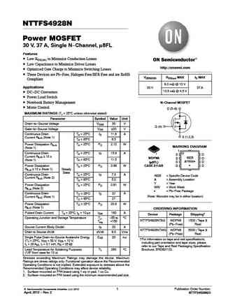
nttfs4800n-d.pdf

NTTFS4800N Power MOSFET 30 V, 32 A, Single N-Channel, m8FL Features Low RDS(on) to Minimize Conduction Losses Low Capacitance to Minimize Driver Losses Optimized Gate Charge to Minimize Switching Losses http //onsemi.com These Devices are Pb-Free, Halogen Free/BFR Free and are RoHS Compliant V(BR)DSS RDS(on) MAX ID MAX Applications 20 mW @ 10 V DC-DC Converters
Otros transistores... NTS2101PT1, NTS4001NT1, NTS4101PT1, NTS4172NT1G, NTS4173PT1G, NTS4409N, NTTD4401FR2, NTTFS3A08PZ, AO4407A, NTTFS4821NTAG, NTTFS4823NTAG, NTTFS4824NTAG, NTTFS4928NTAG, NTTFS4929NTAG, NTTFS4930NTAG, NTTFS4932NTAG, NTTFS4937NTAG
Parámetros del MOSFET. Cómo se afectan entre sí.
History: FDD5810F085 | NTP22N06 | IRF840ALPBF | HFS8N70U | NTP5411NG | 3N80G-TMS4-R | DHS020N88E
🌐 : EN ES РУ

Liste
Recientemente añadidas las descripciónes de los transistores:
MOSFET: CS95118 | CS85105A | CS75N45 | CS72N12 | CS55N50 | CS48N75A | CS40N27 | MSQ60P04D | MSQ40P07D | MSQ30P40D | MSQ30P15 | MSQ30P07D | MSQ100N03D | MSHM60P14 | MSHM40N085 | MSHM30N46
Popular searches
2sd330 replacement | a1273 transistor | 2sc1384 equivalent | 2sd786 | a940 transistor | 2sc1815 replacement | 2sc2383 | c3198 transistor