65N06A MOSFET Equivalente. Reemplazo. Hoja de especificaciones. Principales características
Número de Parte: 65N06A
Tipo de FET: MOSFET
Polaridad de transistor: N
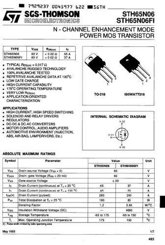
ESPECIFICACIONES MÁXIMAS
Pdⓘ - Máxima
disipación de potencia: 150 W
|Vds|ⓘ - Voltaje máximo drenador-fuente: 55 V
|Vgs|ⓘ - Voltaje máximo fuente-puerta: 20 V
|Id|ⓘ - Corriente continua
de drenaje: 63 A
Tjⓘ - Temperatura máxima de unión: 175 °C
CARACTERÍSTICAS ELÉCTRICAS
trⓘ - Tiempo
de subida: 30 nS
Cossⓘ - Capacitancia de salida: 370 pF
RDSonⓘ - Resistencia estado encendido drenaje a fuente: 0.018 Ohm
Encapsulados: TO-220AB
Búsqueda de reemplazo de 65N06A MOSFET
- Selecciónⓘ de transistores por parámetros
65N06A datasheet
..1. Size:618K nell
65n06a 65n06h.pdf 
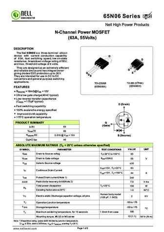
RoHS 65N06 Series RoHS SEMICONDUCTOR Nell High Power Products N-Channel Power MOSFET (63A, 55Volts) DESCRIPTION The Nell 65N06 is a three-terminal silicon device with current conduction capability D of 63A, fast switching speed, low on-state D resistance, breakdown voltage rating of 55V, and max. threshold voltage of 4 volts. They are designed as an extremely efficient G a
9.2. Size:56K philips
phb65n06lt.pdf
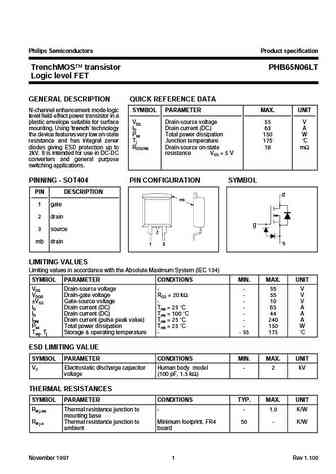
Philips Semiconductors Product specification TrenchMOS transistor PHB65N06LT Logic level FET GENERAL DESCRIPTION QUICK REFERENCE DATA N-channel enhancement mode logic SYMBOL PARAMETER MAX. UNIT level field-effect power transistor in a plastic envelope suitable for surface VDS Drain-source voltage 55 V mounting. Using trench technology ID Drain current (DC) 63 A the device fea
9.3. Size:58K philips
php65n06lt 2.pdf
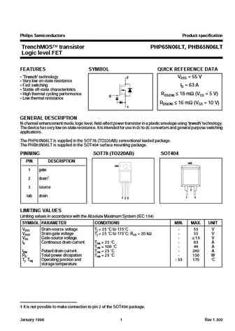
Philips Semiconductors Product specification TrenchMOS transistor PHP65N06LT, PHB65N06LT Logic level FET FEATURES SYMBOL QUICK REFERENCE DATA Trench technology VDSS = 55 V d Very low on-state resistance Fast switching ID = 63 A Stable off-state characteristics High thermal cycling performance RDS(ON) 18 m (VGS = 5 V) g Low thermal resistance
9.4. Size:52K philips
php65n06t 1.pdf
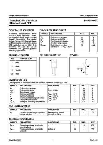
Philips Semiconductors Product specification TrenchMOS transistor PHP65N06T Standard level FET GENERAL DESCRIPTION QUICK REFERENCE DATA N-channel enhancement mode SYMBOL PARAMETER MAX. UNIT standard level field-effect power transistor in a plastic envelope using VDS Drain-source voltage 55 V trench technology. The device ID Drain current (DC) 63 A features very low on-state r
9.5. Size:55K philips
phb65n06t 1.pdf
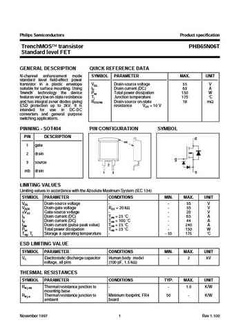
Philips Semiconductors Product specification TrenchMOS transistor PHB65N06T Standard level FET GENERAL DESCRIPTION QUICK REFERENCE DATA N-channel enhancement mode SYMBOL PARAMETER MAX. UNIT standard level field-effect power transistor in a plastic envelope VDS Drain-source voltage 55 V suitable for surface mounting. Using ID Drain current (DC) 63 A trench technology the devic
9.6. Size:661K fairchild semi
fqp65n06.pdf
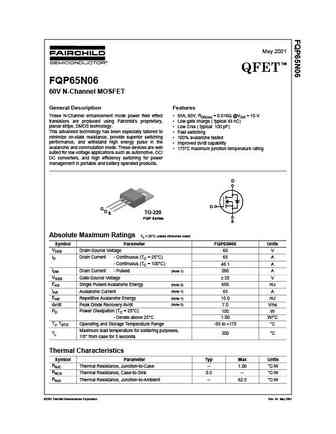
May 2001 TM QFET FQP65N06 60V N-Channel MOSFET General Description Features These N-Channel enhancement mode power field effect 65A, 60V, RDS(on) = 0.016 @VGS = 10 V transistors are produced using Fairchild s proprietary, Low gate charge ( typical 48 nC) planar stripe, DMOS technology. Low Crss ( typical 100 pF) This advanced technology has been especially tailored to
9.7. Size:651K fairchild semi
fqa65n06.pdf
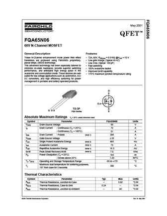
May 2001 TM QFET FQA65N06 60V N-Channel MOSFET General Description Features These N-Channel enhancement mode power field effect 72A, 60V, RDS(on) = 0.016 @VGS = 10 V transistors are produced using Fairchild s proprietary, Low gate charge ( typical 48 nC) planar stripe, DMOS technology. Low Crss ( typical 100 pF) This advanced technology has been especially tailored to
9.8. Size:668K fairchild semi
fqb65n06 fqi65n06.pdf
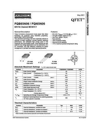
May 2001 TM QFET FQB65N06 / FQI65N06 60V N-Channel MOSFET General Description Features These N-Channel enhancement mode power field effect 65A, 60V, RDS(on) = 0.016 @VGS = 10 V transistors are produced using Fairchild s proprietary, Low gate charge ( typical 48 nC) planar stripe, DMOS technology. Low Crss ( typical 100 pF) This advanced technology has been especially
9.9. Size:666K fairchild semi
fqb65n06tm.pdf

May 2001 TM QFET FQB65N06 / FQI65N06 60V N-Channel MOSFET General Description Features These N-Channel enhancement mode power field effect 65A, 60V, RDS(on) = 0.016 @VGS = 10 V transistors are produced using Fairchild s proprietary, Low gate charge ( typical 48 nC) planar stripe, DMOS technology. Low Crss ( typical 100 pF) This advanced technology has been especially
9.10. Size:681K fairchild semi
fqpf65n06.pdf
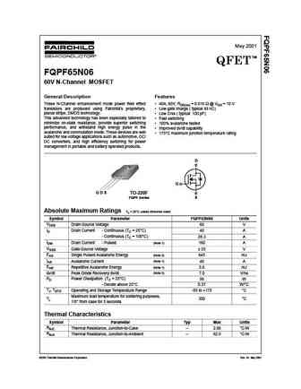
May 2001 TM QFET FQPF65N06 60V N-Channel MOSFET General Description Features These N-Channel enhancement mode power field effect 40A, 60V, RDS(on) = 0.016 @ VGS = 10 V transistors are produced using Fairchild s proprietary, Low gate charge ( typical 48 nC) planar stripe, DMOS technology. Low Crss ( typical 100 pF) This advanced technology has been especially tailored
9.11. Size:652K fairchild semi
fqaf65n06.pdf

May 2001 TM QFET FQAF65N06 60V N-Channel MOSFET General Description Features These N-Channel enhancement mode power field effect 49A, 60V, RDS(on) = 0.016 @VGS = 10 V transistors are produced using Fairchild s proprietary, Low gate charge ( typical 48 nC) planar stripe, DMOS technology. Low Crss ( typical 100 pF) This advanced technology has been especially tailored t
9.12. Size:598K fairchild semi
fdp65n06.pdf
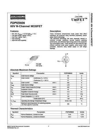
June 2006 TM UniFET FDP65N06 60V N-Channel MOSFET Features Description 65A, 60V, RDS(on) = 0.016 @VGS = 10 V These N-Channel enhancement mode power field effect Low gate charge ( typical 132nC) transistors are produced using Fairchild s proprietary, planar stripe, DMOS technology. Low Crss ( typical 35pF) This advanced technology has been especially tailored to
9.13. Size:548K samsung
sfp65n06.pdf
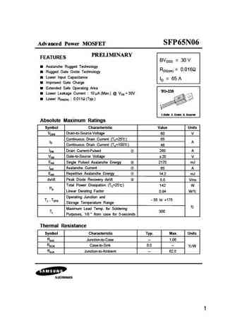
Advanced Power MOSFET PRELIMINARY FEATURES BVDSS = 30 V Avalanche Rugged Technology RDS(on) = 0.016 Rugged Gate Oxide Technology Lower Input Capacitance ID = 65 A Improved Gate Charge Extended Safe Operating Area TO-220 Lower Leakage Current 10 A (Max.) @ VDS = 30V Lower RDS(ON) 0.011 (Typ.) 1 2 3 1.Gate 2. Drain 3. Source Absolute Maximum Ratings Symbol Characte
9.14. Size:172K rohm
rsh065n06tb1.pdf

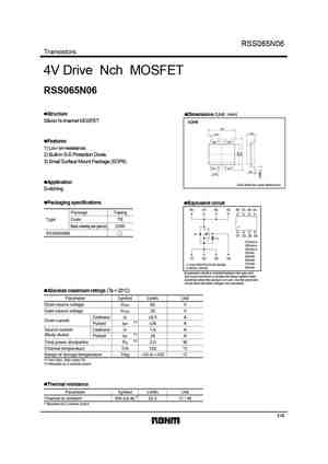
4V Drive Nch MOSFET RSH065N06 Structure Dimensions (Unit mm) Silicon N-channel MOSFET SOP8 Features 1) Low on-resistance. 2) Built-in G-S Protection Diode. 3) Small Surface Mount Package (SOP8). Application Switching Each lead has same dimensions Packaging specifications Inner circuit (8) (7) (6) (5) (8) (7) (6) (5) Package Taping Type Code TB Basi
9.15. Size:97K rohm
rss065n06fu6tb.pdf
RSS065N06 Transistors 4V Drive Nch MOSFET RSS065N06 Structure Dimensions (Unit mm) Silicon N-channel MOSFET SOP8 Features 1) Low on-resistance. 2) Built-in G-S Protection Diode. 3) Small Surface Mount Package (SOP8). Application Each lead has same dimensions Switching Packaging specifications Equivalent circuit (8) (7) (6) (5) (8) (7) (6) (5) Package Tapi
9.16. Size:173K rohm
rsh065n06.pdf
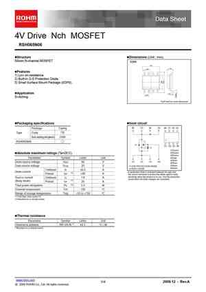
4V Drive Nch MOSFET RSH065N06 Structure Dimensions (Unit mm) Silicon N-channel MOSFET SOP8 Features 1) Low on-resistance. 2) Built-in G-S Protection Diode. 3) Small Surface Mount Package (SOP8). Application Switching Each lead has same dimensions Packaging specifications Inner circuit (8) (7) (6) (5) (8) (7) (6) (5) Package Taping Type Code TB Basi
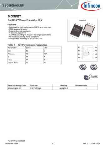
9.17. Size:1445K infineon
bsz065n06ls5.pdf
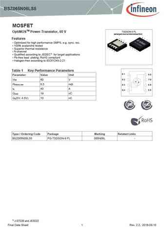
BSZ065N06LS5 MOSFET TSDSON-8 FL OptiMOSTM Power-Transistor, 60 V (enlarged source interconnection) Features Optimized for high performance SMPS, e.g. sync. rec. 100% avalanche tested Superior thermal resistance N-channel Qualified according to JEDEC1) for target applications Pb-free lead plating; RoHS compliant Halogen-free according to IEC61249-2-21 Tab
9.18. Size:738K infineon
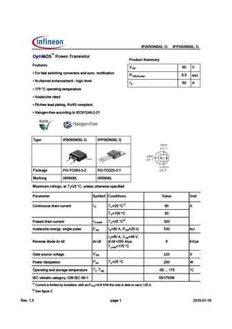
ipb065n06lg ipp065n06lg.pdf
IPB065N06L G IPP065N06L G Power-Transistor Product Summary Features V D P ?A 61BC BF9C389>7 3?>E5AC5AB 1>4 BH>3 A53C96931C9?> R m , ?> =1G P ( 381>>581>35=5>C
9.19. Size:1307K infineon
bsc065n06ls5.pdf
BSC065N06LS5 MOSFET SuperSO8 OptiMOSTM Power-Transistor, 60 V 5 8 6 7 Features 7 6 8 5 Optimized for high performance SMPS, e.g. sync. rec. 100% avalanche tested Superior thermal resistance N-channel, logic level 4 Qualified according to JEDEC1) for target applications 1 3 2 2 Pb-free lead plating; RoHS compliant 3 1 4 Halogen-free according t
9.20. Size:801K onsemi
fqp65n06.pdf

Is Now Part of To learn more about ON Semiconductor, please visit our website at www.onsemi.com Please note As part of the Fairchild Semiconductor integration, some of the Fairchild orderable part numbers will need to change in order to meet ON Semiconductor s system requirements. Since the ON Semiconductor product management systems do not have the ability to manage part nomenclatur
9.21. Size:587K onsemi
fqpf65n06.pdf

Is Now Part of To learn more about ON Semiconductor, please visit our website at www.onsemi.com Please note As part of the Fairchild Semiconductor integration, some of the Fairchild orderable part numbers will need to change in order to meet ON Semiconductor s system requirements. Since the ON Semiconductor product management systems do not have the ability to manage part nomenclatur
9.22. Size:1167K onsemi
fdp65n06.pdf

Is Now Part of To learn more about ON Semiconductor, please visit our website at www.onsemi.com Please note As part of the Fairchild Semiconductor integration, some of the Fairchild orderable part numbers will need to change in order to meet ON Semiconductor s system requirements. Since the ON Semiconductor product management systems do not have the ability to manage part nomenclatur
9.23. Size:1036K cn wxdh
dh065n06 dh065n06e.pdf
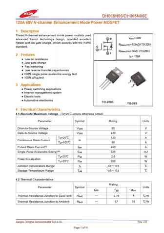
DH065N06/DH065N06E 120A 60V N-channel Enhancement Mode Power MOSFET 1 Description These N-channel enhancement mode power mosfets used V = 60V DSS 2 D advanced trench technology design, provided excellent Rdson and low gate charge. Which accords with the RoHS R = 5.2m TO-220 DS(on) (TYP) standard. G 1 R = 5m TO-263 DS(on) (TYP) 3 S 2 Features I = 120A D Low
9.24. Size:855K cn wxdh
dh065n06d.pdf
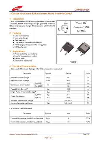
DH065N06D 110A 60V N-channel Enhancement Mode Power MOSFET 1 Description These N-channel enhancement mode power mosfets used V = 60V 2 D DSS advanced trench technology design, provided excellent Rdson and low gate charge. Which accords with the RoHS R = 5m DS(on) (TYP) standard. G 1 I = 110A D 3 S 2 Features Low on resistance Low gate charge Fast switching L
9.25. Size:850K cn vbsemi
rss065n06.pdf
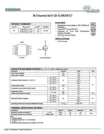
RSS065N06 www.VBsemi.tw N-Channel 60-V (D-S) MOSFET FEATURES PRODUCT SUMMARY Halogen-free According to IEC 61249-2-21 VDS (V) RDS(on) ( ) ID (A)d Qg (Typ.) Definition TrenchFET Power MOSFET 0.025 at VGS = 10 V 7.6 60 10.5 nC Optimized for Low Side Synchronous 0.030 at VGS = 4.5 V 6.5 Rectifier Operation 100 % Rg and UIS Tested APPLICATIONS D CCFL
9.26. Size:230K inchange semiconductor
65n06.pdf
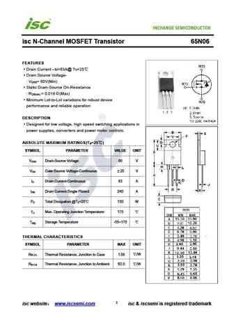
isc N-Channel MOSFET Transistor 65N06 FEATURES Drain Current I =63A@ T =25 D C Drain Source Voltage- V = 60V(Min) DSS Static Drain-Source On-Resistance R = 0.018 (Max) DS(on) Minimum Lot-to-Lot variations for robust device performance and reliable operation DESCRIPTION Designed for low voltage, high speed switching applications in power supplies, converters an
9.27. Size:1817K cn apm
ap65n06df.pdf
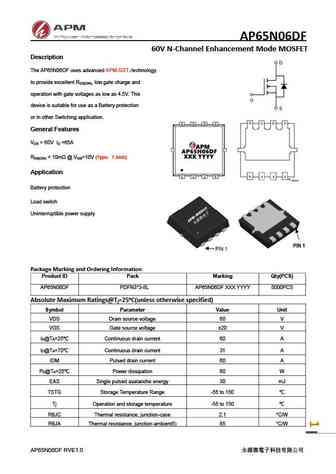
AP65N06DF 60V N-Channel Enhancement Mode MOSFET Description The AP65N06DF uses advanced APM-SGT technology to provide excellent R , low gate charge and DS(ON) operation with gate voltages as low as 4.5V. This device is suitable for use as a Battery protection or in other Switching application. General Features V = 60V I =65A DS D R
9.28. Size:1552K cn apm
ap65n06nf.pdf
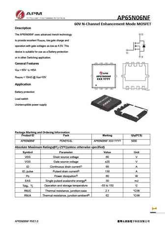
AP65N06NF 60V N-Channel Enhancement Mode MOSFET Description The AP65N06NF uses advanced trench technology to provide excellent R , low gate charge and DS(ON) operation with gate voltages as low as 4.5V. This device is suitable for use as a Battery protection or in other Switching application. General Features V = 60V I =65A DS D R
9.29. Size:1844K cn apm
ap65n06d.pdf
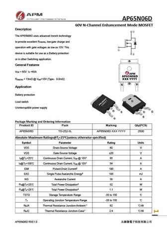
AP65N06D 60V N-Channel Enhancement Mode MOSFET Description The AP65N06D uses advanced trench technology to provide excellent R , low gate charge and DS(ON) operation with gate voltages as low as 10V. This device is suitable for use as a Battery protection or in other Switching application. General Features V = 60V I =65A DS D R
Otros transistores... 5N60AF, 5N60G, 5N65A, 5N65AF, 5N65F, 5N65G, 5N90A, 5N90AF, IRFP250, 65N06H, 6680A, 6HP04CH, 6HP04MH, 6LN04SS, 6N60A, 6N60AF, 6N60F