DE275-501N16A Datasheet. Equivalente. Reemplazo. Hoja de especificaciones. Principales características
Número de Parte: DE275-501N16A 📄📄
Tipo de FET: MOSFET
Polaridad de transistor: N
ESPECIFICACIONES MÁXIMAS
Pdⓘ - Máxima disipación de potencia: 590 W
|Vds|ⓘ - Voltaje máximo drenador-fuente: 500 V
|Vgs|ⓘ - Voltaje máximo fuente-puerta: 20 V
|Id|ⓘ - Corriente continua de drenaje: 16 A
Tjⓘ - Temperatura máxima de unión: 175 °C
CARACTERÍSTICAS ELÉCTRICAS
Cossⓘ - Capacitancia de salida: 122 pF
RDSonⓘ - Resistencia estado encendido drenaje a fuente: 0.4 Ohm
Encapsulados: DE275
📄📄 Copiar
Búsqueda de reemplazo de DE275-501N16A MOSFET
- Selecciónⓘ de transistores por parámetros
DE275-501N16A datasheet
de275-501n16a.pdf
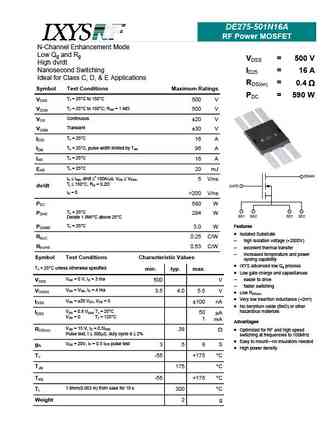
DE275-501N16A RF Power MOSFET N-Channel Enhancement Mode Low Qg and Rg VDSS = 500 V High dv/dt Nanosecond Switching ID25 = 16 A Ideal for Class C, D, & E Applications RDS(on) = 0.4 Symbol Test Conditions Maximum Ratings PDC = 590 W TJ = 25 C to 150 C VDSS 500 V TJ = 25 C to 150 C; RGS = 1 M VDGR 500 V Continuous VGS 20 V Transien
de275-201n25a.pdf
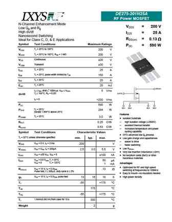
DE275-201N25A RF Power MOSFET N-Channel Enhancement Mode VDSS = 200 V Low Qg and Rg High dv/dt ID25 = 25 A Nanosecond Switching RDS(on) = 0.13 Ideal for Class C, D, & E Applications Symbol Test Conditions Maximum Ratings PDC = 590 W TJ = 25 C to 150 C VDSS 200 V TJ = 25 C to 150 C; RGS = 1 M VDGR 200 V Continuous VGS 20 V Transie
de275-102n06a.pdf
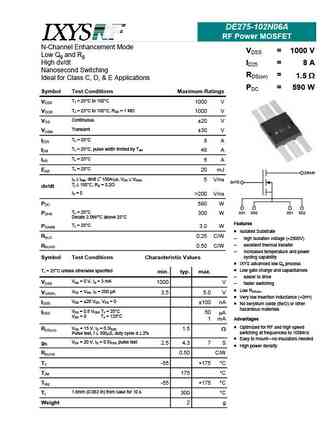
DE275-102N06A RF Power MOSFET N-Channel Enhancement Mode VDSS = 1000 V Low Qg and Rg High dv/dt ID25 = 8 A Nanosecond Switching RDS(on) = 1.5 Ideal for Class C, D, & E Applications PDC = 590 W Symbol Test Conditions Maximum Ratings TJ = 25 C to 150 C VDSS 1000 V TJ = 25 C to 150 C; RGS = 1 M VDGR 1000 V Continuous VGS 20 V Transi
de275-101n30a.pdf
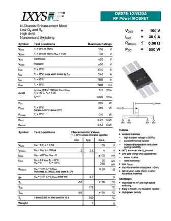
DE275-101N30A RF Power MOSFET N-Channel Enhancement Mode Low Qg and Rg VDSS = 100 V High dv/dt ID25 = 30.0 A Nanosecond Switching RDS(on) Symbol Test Conditions Maximum Ratings 0.06 TJ = 25 C to 150 C VDSS 100 V PDC = 550 W TJ = 25 C to 150 C; RGS = 1 M VDGR 100 V Continuous VGS 20 V Transient VGSM 30 V Tc = 25 C ID25 30
Otros transistores... D84DN2, DE150-101N09A, DE150-102N02A, DE150-201N09A, DE150-501N04A, DE275-101N30A, DE275-102N06A, DE275-201N25A, P60NF06, DE275X2-102N06A, DE275X2-501N16A, DE375-102N10A, DE375-102N12A, DE375-501N21A, DE475-102N20A, DE475-102N21A, DE475-501N44A
History: SVG108R5NAM | SVG108R5NAMJ
🌐 : EN ES РУ

Liste
Recientemente añadidas las descripciónes de los transistores:
MOSFET: BCD70N07A | BCD90N03 | BCD80N06 | T50N06 | H50N06 | BCD12N65 | BCT12N65 | BCD4N65 | BCT4N65 | BCD7N65 | BCT7N65 | BCT20N65 | ASDM30P100KQ | ASDM30N90Q | ASDM30N75KQ | ASDM30N150Q
Popular searches
a1013 transistor | 2sc2705 | bc239 | 2sc3264 | mp38a | bc546 transistor | bd243 | 2sk170 datasheet