DMP1011UCB9 MOSFET Equivalente. Reemplazo. Hoja de especificaciones. Principales características
Número de Parte: DMP1011UCB9
Tipo de FET: MOSFET
Polaridad de transistor: P
ESPECIFICACIONES MÁXIMAS
Pdⓘ - Máxima
disipación de potencia: 0.89 W
|Vds|ⓘ - Voltaje máximo drenador-fuente: 8 V
|Vgs|ⓘ - Voltaje máximo fuente-puerta: 6 V
|Id|ⓘ - Corriente continua
de drenaje: 10 A
Tjⓘ - Temperatura máxima de unión: 150 °C
CARACTERÍSTICAS ELÉCTRICAS
trⓘ - Tiempo
de subida: 22.6 nS
Cossⓘ - Capacitancia de salida: 595 pF
RDSonⓘ - Resistencia estado encendido drenaje a fuente: 0.01 Ohm
Encapsulados: U-WLB1515-9
Búsqueda de reemplazo de DMP1011UCB9 MOSFET
- Selecciónⓘ de transistores por parámetros
DMP1011UCB9 datasheet
..1. Size:457K diodes
dmp1011ucb9.pdf 

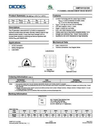
DMP1011UCB9 P-CHANNEL ENHANCEMENT MODE MOSFET Product Summary (Typ. @ VGS = -4.5V, TA = +25 C) Features LD-MOS Technology with the Lowest Figure of Merit VDSS RDS(on) Qg Qgd ID RDS(on) = 8.2m to Minimize On-State Losses -8V 8.2m 8.1nC 1.8nC -10A Qg = 8.1nC for Ultra-Fast Switching Vgs(th) = -0.8V typ. for a Low Turn-On Potential CSP with Footprint 1.5mm 1.5
8.1. Size:232K diodes
dmp1012ucb9.pdf 

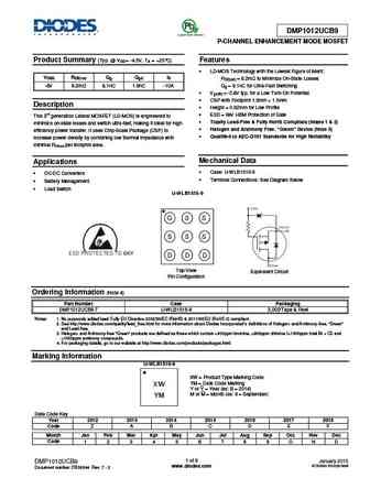
DMP1012UCB9 P-CHANNEL ENHANCEMENT MODE MOSFET Product Summary (Typ. @ VGS = -4.5V, TA = +25 C) Features LD-MOS Technology with the Lowest Figure of Merit VDSS RDS(on) Qg Qgd ID RDS(on) = 8.2m to Minimize On-State Losses -8V 8.2m 8.1nC 1.8nC -10A Qg = 8.1nC for Ultra-Fast Switching Vgs(th) = -0.8V typ. for a Low Turn-On Potential CSP with Footprint 1.5mm 1.
8.2. Size:326K diodes
dmp1018ucb9.pdf 

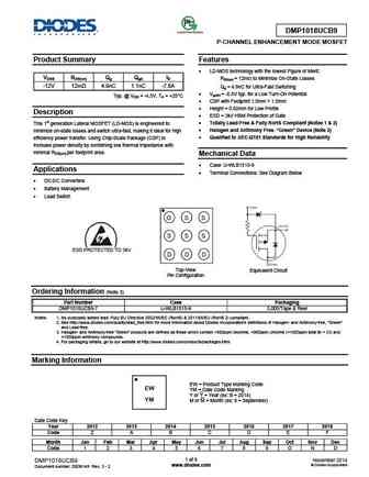
DMP1018UCB9 P-CHANNEL ENHANCEMENT MODE MOSFET Product Summary Features LD-MOS technology with the lowest Figure of Merit VDSS RDS(on) Qg Qgd ID RDS(on) = 12m to Minimize On-State Losses -12V 12m 4.9nC 1.1nC -7.6A Qg = 4.9nC for Ultra-Fast Switching Vgs(th) = -0.8V typ. for a Low Turn-On Potential Typ. @ VGS = -4.5V, TA = +25 C CSP with Footprint 1.5mm 1.5
9.1. Size:479K diodes
dmp10h400sk3.pdf 

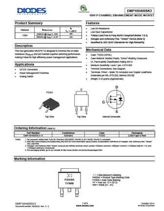
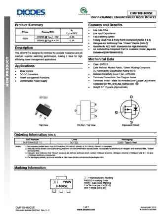
DMP10H400SK3 100V P-CHANNEL ENHANCEMENT MODE MOSFET Product Summary Features ID Low On-Resistance V(BR)DSS RDS(on) max TC = +25 C Low Input Capacitance 240m @ VGS = -10V -9A -100V Totally Lead-Free & Fully RoHS Compliant (Notes 1 & 2) -8A 300m @ VGS = -4.5V Halogen and Antimony Free. Green Device (Note 3) Qualified to AEC-Q101 Standards
9.2. Size:268K diodes
dmp1055ufdb.pdf 

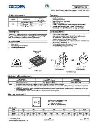
DMP1055UFDB DUAL P-CHANNEL ENHANCEMENT MODE MOSFET Product Summary Features Low On-Resistance ID MAX V(BR)DSS RDS(ON) max Low Input Capacitance TA = +25 C Low Profile, 0.6mm Max Height 59m @ VGS = -4.5V -3.9A ESD protected gate. -12V 81m @ VGS = -2.5V -3.3A Totally Lead-Free & Fully RoHS Compliant (Notes 1 & 2) 115m @ VGS = -1.8V -2.8A
9.3. Size:488K diodes
dmp1005ufdf.pdf 

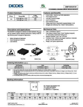
DMP1005UFDF P-CHANNEL ENHANCEMENT MODE MOSFET Product Summary Features and Benefits 0.6mm Profile Ideal for Low Profile Applications ID Max BVDSS RDS(ON) Max PCB Footprint of 4mm2 TC = +25 C 8.5m @ VGS = -4.5V -26A Low Gate Threshold Voltage -12V -22A 12m @ VGS = -2.5V Low On-Resistance ESD Protected up to 8kV Totally Lead-Free &
9.4. Size:533K diodes
dmp10h4d2s.pdf 

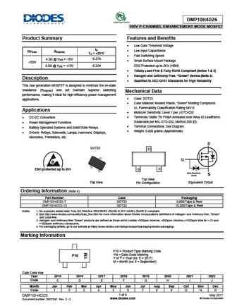
DMP10H4D2S 100V P-CHANNEL ENHANCEMENT MODE MOSFET Product Summary Features and Benefits Low Gate Threshold Voltage ID Low Input Capacitance BVDSS RDS(ON) TA = +25 C Fast Switching Speed 4.2 @ VGS = -10V -0.27A Small Surface Mount Package -100V 5.0 @ VGS = -4.0V -0.24A ESD Protected up to 2KV (HBM) Totally Lead-Free & Fully RoHS Compliant
9.5. Size:189K diodes
dmp1045ufy4.pdf 

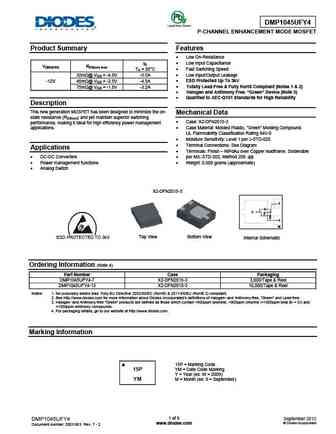
DMP1045UFY4 P-CHANNEL ENHANCEMENT MODE MOSFET Product Summary Features Low On-Resistance ID Low Input Capacitance V(BR)DSS RDS(on) max TA = 25 C Fast Switching Speed 32m @ VGS = -4.5V -5.5A Low Input/Output Leakage -12V 45m @ VGS = -2.5V -4.5A ESD Protected Up To 3kV Totally Lead-Free & Fully RoHS Compliant (Notes 1 & 2) 75m @ VGS = -1.8V -3.2A
9.6. Size:439K diodes
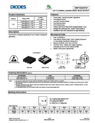
dmp1022ufdf.pdf 

DMP1022UFDF 12V P-CHANNEL ENHANCEMENT MODE MOSFET Product Summary Features ID max 0.6mm profile ideal for low profile applications V(BR)DSS RDS(ON) max TA = +25 C PCB footprint of 4mm2 Low Gate Threshold Voltage 14.8m @ VGS = -4.5V -9.5A Fast Switching Speed 19m @ VGS = -2.5V -8.5A -12V ESD Protected Gate 26m @ VGS = -1.8V -7.2A To
9.7. Size:361K diodes
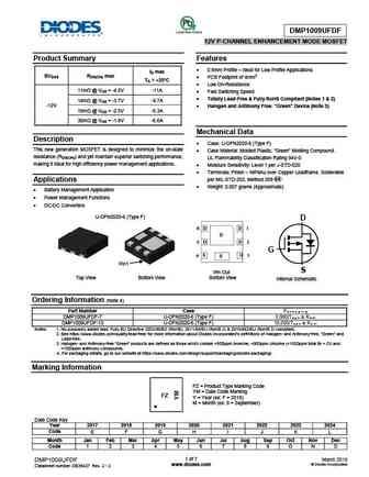
dmp1009ufdf.pdf 

DMP1009UFDF 12V P-CHANNEL ENHANCEMENT MODE MOSFET Product Summary Features 0.6mm Profile Ideal for Low Profile Applications ID max BVDSS RDS(ON) max PCB Footprint of 4mm2 TA = +25 C Low On-Resistance 11m @ VGS = -4.5V -11A Fast Switching Speed Totally Lead-Free & Fully RoHS Compliant (Notes 1 & 2) 14m @ VGS = -3.7V -9.7A -12V Halo
9.8. Size:152K diodes
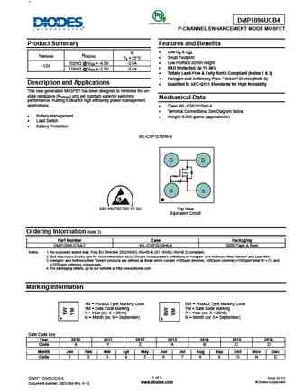
dmp1096ucb4.pdf 

DMP1096UCB4 P-CHANNEL ENHANCEMENT MODE MOSFET Product Summary Features and Benefits Low Qg & Qgd ID V(BR)DSS RDS(ON) Small Footprint TA = 25 C Low Profile 0.62mm height 102m @ VGS = -4.5V -2.6A -12V ESD Protected Up To 3KV 116m @ VGS = -2.5V -2.4A Totally Lead-Free & Fully RoHS Compliant (Notes 1 & 2) Halogen and Antimony Free. Gre
9.9. Size:396K diodes
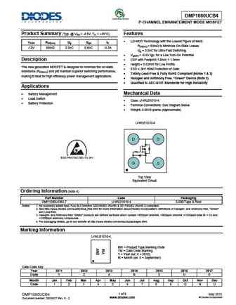
dmp1080ucb4.pdf 

DMP1080UCB4 P-CHANNEL ENHANCEMENT MODE MOSFET Product Summary (Typ. @ VGS = -4.5V, TA = +25 C) Features LD-MOS Technology with the Lowest Figure of Merit VDSS RDS(on) Qg Qgd ID RDS(on) = 65m to Minimize On-State Losses -12V 65m 2.5nC 0.6nC -3.3A Qg = 2.5nC for Ultra-Fast Switching Vgs(th) = -0.6V typ. for a Low Turn-On Potential Description CSP with Footprin
9.10. Size:391K diodes
dmp1045u.pdf 

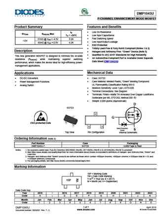
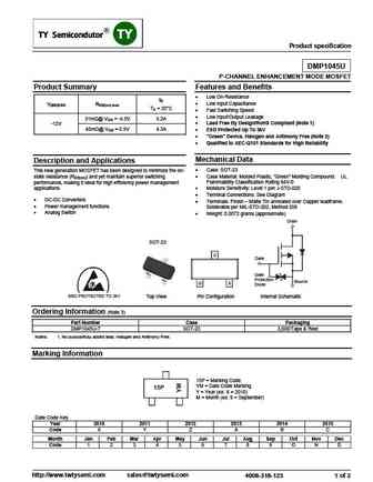
DMP1045U P-CHANNEL ENHANCEMENT MODE MOSFET Product Summary Features and Benefits Low On-Resistance ID BVDSS RDS(ON) Max TA = +25 C Low Input Capacitance Fast Switching Speed 31m @ VGS = -4.5V 5.2A -12V Low Input/Output Leakage 45m @ VGS =-2.5V 4.3A ESD Protected Totally Lead-Free & Fully RoHS Compliant (Notes 1 & 2) Description Ha
9.12. Size:207K diodes
dmp1022ufde.pdf 

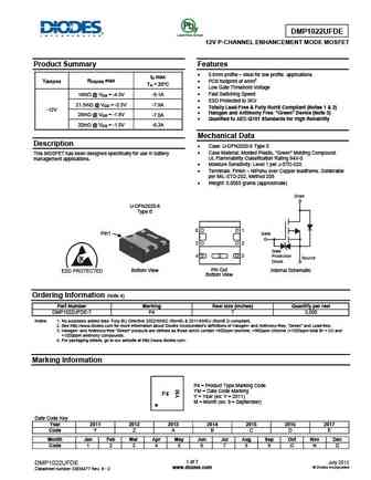
DMP1022UFDE 12V P-CHANNEL ENHANCEMENT MODE MOSFET Product Summary Features 0.6mm profile ideal for low profile applications ID max V(BR)DSS RDS(ON) max PCB footprint of 4mm2 TA = 25 C Low Gate Threshold Voltage Fast Switching Speed 16m @ VGS = -4.5V -9.1A ESD Protected to 3KV 21.5m @ VGS = -2.5V -7.9A Totally Lead-Free & Fully RoHS Comp
9.13. Size:433K diodes
dmp1055usw.pdf 

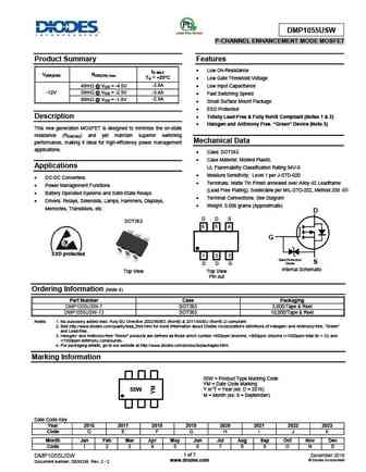
DMP1055USW P-CHANNEL ENHANCEMENT MODE MOSFET Product Summary Features Low On-Resistance ID MAX V(BR)DSS RDS(ON) max TA = +25 C Low Gate Threshold Voltage -3.8A 48m @ VGS = -4.5V Low Input Capacitance -12V -3.4A 59m @ VGS = -2.5V Fast Switching Speed 80m @ VGS = -1.8V -2.9A Small Surface Mount Package ESD Protected Description
9.14. Size:357K diodes
dmp1046ufdb.pdf 

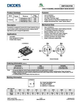
DMP1046UFDB DUAL P-CHANNEL ENHANCEMENT MODE MOSFET Product Summary Features Low On-Resistance ID MAX Device V(BR)DSS RDS(ON) max TA = +25 C Low Input Capacitance Low Profile, 0.6mm Max Height 61m @ VGS = -4.5V -3.8A P-Channel -12V 81m @ VGS = -2.5V -3.3A Totally Lead-Free & Fully RoHS Compliant (Notes 1 & 2) 115m @ VGS = -1.8V -2.8A Halogen and
9.15. Size:404K diodes
dmp10h400seq.pdf 

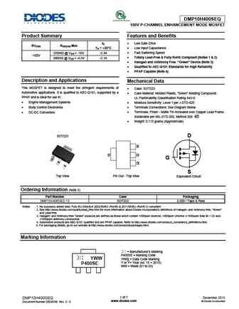
DMP10H400SEQ 100V P-CHANNEL ENHANCEMENT MODE MOSFET Product Summary Features and Benefits ID Low Gate Drive BVDSS RDS(ON) Max TA = +25 C Low Input Capacitance Fast Switching Speed 250m @ VGS = -10V -2.3A -100V Totally Lead-Free & Fully RoHS Compliant (Notes 1 & 2) 300m @ VGS = -4.5V -2.1A Halogen and Antimony Free. Green Device (Note 3)
9.16. Size:81K tysemi
dmp1045u.pdf 

Product specification DMP1045U P-CHANNEL ENHANCEMENT MODE MOSFET Product Summary Features and Benefits Low On-Resistance ID Low Input Capacitance V(BR)DSS RDS(on) max TA = 25 C Fast Switching Speed Low Input/Output Leakage 31m @ VGS = -4.5V 5.2A Lead Free By Design/RoHS Compliant (Note 1) -12V 4.3A 45m @ VGS =-2.5V ESD Protected Up To
9.17. Size:266K inchange semiconductor
dmp10h400sk3.pdf 
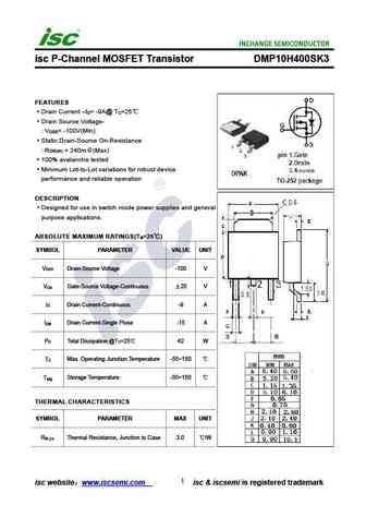
isc P-Channel MOSFET Transistor DMP10H400SK3 FEATURES Drain Current I = -9A@ T =25 D C Drain Source Voltage- V = -100V(Min) DSS Static Drain-Source On-Resistance R = 240m (Max) DS(on) 100% avalanche tested Minimum Lot-to-Lot variations for robust device performance and reliable operation DESCRIPTION Designed for use in switch mode power supplies and general
Otros transistores... DMN62D1LFD, DMN63D8LDW, DMN63D8LV, DMN65D8L, DMN65D8LDW, DMN65D8LFB, DMN65D8LW, DMN7022LFG, IRFZ44, DMP1012UCB9, DMP1018UCB9, DMP1022UFDE, DMP1022UFDF, DMP1045UFY4, DMP1046UFDB, DMP1055UFDB, DMP1080UCB4
