DMP22D4UFA MOSFET Equivalente. Reemplazo. Hoja de especificaciones. Principales características
Número de Parte: DMP22D4UFA
Tipo de FET: MOSFET
Polaridad de transistor: P
ESPECIFICACIONES MÁXIMAS
Pdⓘ - Máxima disipación de potencia: 0.4 W
|Vds|ⓘ - Voltaje máximo drenador-fuente: 20 V
|Vgs|ⓘ - Voltaje máximo fuente-puerta: 8 V
|Id|ⓘ - Corriente continua de drenaje: 0.33 A
Tjⓘ - Temperatura máxima de unión: 150 °C
CARACTERÍSTICAS ELÉCTRICAS
trⓘ - Tiempo de subida: 5.7 nS
Cossⓘ - Capacitancia de salida: 4.2 pF
RDSonⓘ - Resistencia estado encendido drenaje a fuente: 1.9 Ohm
Encapsulados: DFN0806H4-3
Búsqueda de reemplazo de DMP22D4UFA MOSFET
- Selecciónⓘ de transistores por parámetros
DMP22D4UFA datasheet
dmp22d4ufa.pdf
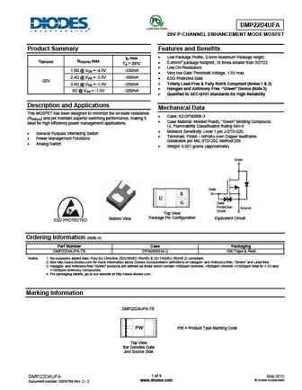
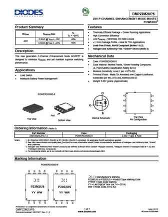
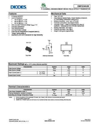
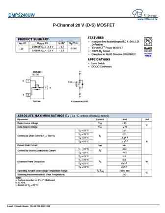
DMP22D4UFA 20V P-CHANNEL ENHANCEMENT MODE MOSFET Product Summary Features and Benefits Low Package Profile, 0.4mm Maximum Package height ID max V(BR)DSS RDS(ON) max 0.48mm2 package footprint, 16 times smaller than SOT23 TA = 25 C Low On-Resistance 1.9 @ VGS = -4.5V -330mA Very low Gate Threshold Voltage, 1.0V max 2.4 @ VGS = -2.5V -300mA ESD Prot
dmp22d6ut.pdf
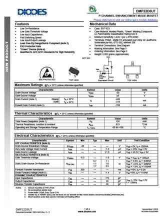
DMP22D6UT P-CHANNEL ENHANCEMENT MODE MOSFET Please click here to visit our online spice models database. Features Mechanical Data Low On-Resistance Case SOT-523 Low Gate Threshold Voltage Case Material Molded Plastic, Green Molding Compound. UL Flammability Classification Rating 94V-0 Low Input Capacitance Moisture Sensitivity Level 1 per J-STD-020D
dmp22m2ups-13.pdf
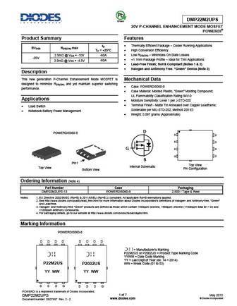
DMP22M2UPS Green 20V P-CHANNEL ENHANCEMENT MODE MOSFET POWERDI Product Summary Features ID Thermally Efficient Package Cooler Running Applications BVDSS RDS(ON) max TC = +25 C High Conversion Efficiency Low RDS(ON) Minimizes On State Losses 2.5m @ VGS = -10V -60A -20V
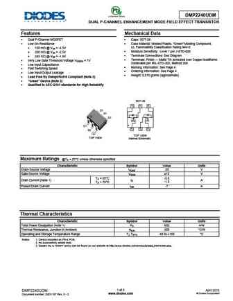
dmp2200ufcl.pdf
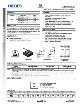
DMP2200UFCL Dual P-CHANNEL ENHANCEMENT MODE MOSFET Summary Features Typical off board profile of 0.5mm - ideally suited for thin V(BR)DSS RDS(on) max ID max applications 200m @VGS = -4.5V -1.7 A Low RDS(ON) minimizes conduction losses 290m @VGS = -2.5V -1.3 A -20V PCB footprint of 2.56mm2 390m @VGS = -1.8V -1.1 A Totally Lead-Free & Fully RoHS Co
Otros transistores... DMP21D0UFD, DMP21D0UT, DMP21D2UFA, DMP21D5UFB4, DMP21D5UFD, DMP2200UDW, DMP2200UFCL, DMP2240UWQ, NCEP15T14, DMP22M2UPS, DMP2305UVT, DMP2540UCB9, DMP25H18DLFDE, DMP26M7UFG, DMP3008SFG, DMP3010LK3, DMP3010LPSQ
History: DMP3017SFGQ
🌐 : EN ES РУ

Liste
Recientemente añadidas las descripciónes de los transistores:
MOSFET: FTF30P35D | FTF25N35DHVT | FTF15N35D | FTE15C35G | FTP02P15G | FTE02P15G | AKF30N5P0SX | AKF30N10S | AKF20P45D | CM4407 | CM3407 | CM3400 | SVF11N65F | SVF11N65T | FKBB3105 | EHBA036R1
Popular searches
c2482 transistor | 2sc1222 replacement | 2sa725 | c5242 transistor | 2sa726 replacement | a1941 datasheet | hrf3205 | c2837 datasheet