2N60AF MOSFET Equivalente. Reemplazo. Hoja de especificaciones. Principales características
Número de Parte: 2N60AF
Tipo de FET: MOSFET
Polaridad de transistor: N
ESPECIFICACIONES MÁXIMAS
Pdⓘ - Máxima disipación de potencia: 23 W
|Vds|ⓘ - Voltaje máximo drenador-fuente: 600 V
|Vgs|ⓘ - Voltaje máximo fuente-puerta: 30 V
|Id|ⓘ - Corriente continua de drenaje: 2 A
Tjⓘ - Temperatura máxima de unión: 150 °C
CARACTERÍSTICAS ELÉCTRICAS
trⓘ - Tiempo de subida: 25 nS
Cossⓘ - Capacitancia de salida: 40 pF
RDSonⓘ - Resistencia estado encendido drenaje a fuente: 5 Ohm
Encapsulados: TO-220F
Búsqueda de reemplazo de 2N60AF MOSFET
- Selecciónⓘ de transistores por parámetros
2N60AF datasheet
2n60a 2n60af 2n60g.pdf
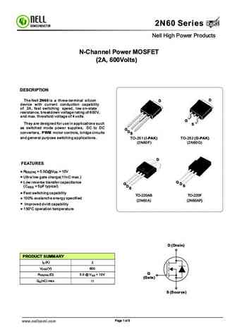
RoHS 2N60 Series RoHS SEMICONDUCTOR Nell High Power Products N-Channel Power MOSFET (2A, 600Volts) DESCRIPTION D The Nell 2N60 is a three-terminal silicon D device with current conduction capability of 2A, fast switching speed, low on-state resistance, breakdown voltage rating of 600V, and max. threshold voltage of 4 volts. G They are designed for use in applications such
12n60a 12n60af.pdf
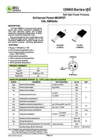
RoHS I2N60 Series RoHS SEMICONDUCTOR Nell High Power Products N-Channel Power MOSFET 12A, 600Volts DESCRIPTION The Nell 12N60 is a three-terminal silicon device with current conduction capability of D 12A, fast switching speed, low on-state resistance, breakdown voltage rating of 600V, and max. threshold voltage of 4 volts. They are designed for use in applications such as s
cm12n60af.pdf
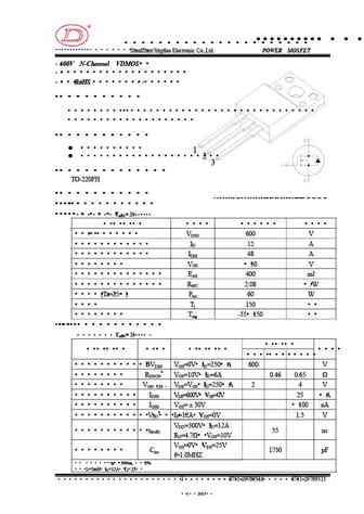
R CM12N60AF www.jdsemi.cn ShenZhen Jingdao Electronic Co.,Ltd. POWER MOSFET 600V N-Channel VDMOS RoHS 1 LD E 2 1
fir2n60afg.pdf
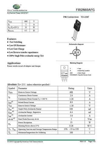
FIR2N60AFG N-Channel Power MOSFET PIN Connection TO-220F VDSS 600 V ID 2 A PD (TC=25 ) 35 W RDS(ON) 4.5 G Features D S Fast Switching g Schematic dia ram Low ON Resistance D Low Gate Charge Low Reverse transfer capacitances G 100% Single Pulse avalanche energy Test S Marking Diagram Applications Power switch circuit of adaptor and charger. Y = Year
Otros transistores... SVS5N70MJ , SVS5N70MN , SVS5N70F , SVS5N70MU , WFP85N06 , 2N5653 , 2N5654 , 2N60A , 2N7000 , 2N60G , 2N6568 , 2N6659-2 , 2N6659X , 2N6660-2 , 2N6660C4A , 2N6660CSM4 , 2N6661-2 .
History: WMN13N50C4 | WMO05N80M3 | WML9N90D1B | WMM08N70EM | WMM36N65F2 | CS55N25A8R-G
History: WMN13N50C4 | WMO05N80M3 | WML9N90D1B | WMM08N70EM | WMM36N65F2 | CS55N25A8R-G
🌐 : EN ES РУ

Liste
Recientemente añadidas las descripciónes de los transistores:
MOSFET: AUB034N10 | AUB033N08BG | AUB026N085 | AUA062N08BG | AUA060N08AG | AUA056N08BGL | AUA039N10 | ASW80R290E | ASW65R120EFD | ASW65R110E | ASW65R095EFD | ASW65R046EFD | ASW65R041EFDA | ASW65R041E | ASW60R150E | ASW60R090EFDA
Popular searches
ao3407 datasheet | c1841 transistor | fb42n20d | irfb3306 equivalent | irfp460 характеристики | k2837 datasheet | k389 transistor | mje15032g equivalent