1N60E MOSFET Equivalente. Reemplazo. Hoja de especificaciones. Principales características
Número de Parte: 1N60E
Tipo de FET: MOSFET
Polaridad de transistor: N
ESPECIFICACIONES MÁXIMAS
Pdⓘ - Máxima
disipación de potencia: 1 W
|Vds|ⓘ - Voltaje máximo drenador-fuente: 600 V
|Vgs|ⓘ - Voltaje máximo fuente-puerta: 30 V
|Id|ⓘ - Corriente continua
de drenaje: 0.3 A
Tjⓘ - Temperatura máxima de unión: 150 °C
CARACTERÍSTICAS ELÉCTRICAS
trⓘ - Tiempo
de subida: 25 nS
Cossⓘ - Capacitancia de salida: 20 pF
RDSonⓘ - Resistencia estado encendido drenaje a fuente: 11.5 Ohm
Encapsulados: TO-92
Búsqueda de reemplazo de 1N60E MOSFET
- Selecciónⓘ de transistores por parámetros
1N60E datasheet
..1. Size:596K nell
1n60af 1n60e 1n60f 1n60g.pdf 
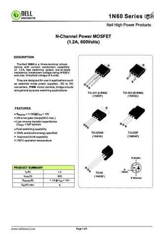
RoHS 1N60 Series RoHS SEMICONDUCTOR Nell High Power Products N-Channel Power MOSFET (1.2A, 600Volts) DESCRIPTION The Nell 1N60 is a three-terminal silicon D D device with current conduction capability of 1.2A, fast switching speed, low on-state resistance, breakdown voltage rating of 600V, and max. threshold voltage of 4 volts. G They are designed for use in applications suc
0.1. Size:266K motorola
mtd1n60e.pdf
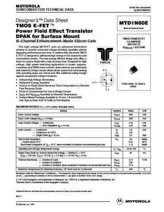
MOTOROLA Order this document SEMICONDUCTOR TECHNICAL DATA by MTD1N60E/D Designer's Data Sheet MTD1N60E TMOS E-FET. Motorola Preferred Device Power Field Effect Transistor DPAK for Surface Mount TMOS POWER FET N Channel Enhancement Mode Silicon Gate 1.0 AMPERE 600 VOLTS This high voltage MOSFET uses an advanced termination RDS(on) = 8.0 OHM scheme to provide enhanced vol
0.2. Size:232K motorola
mtp1n60erev1x.pdf

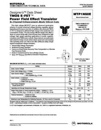
MOTOROLA Order this document SEMICONDUCTOR TECHNICAL DATA by MTP1N60E/D Designer's Data Sheet MTP1N60E TMOS E-FET. Motorola Preferred Device Power Field Effect Transistor N Channel Enhancement Mode Silicon Gate TMOS POWER FET This high voltage MOSFET uses an advanced termination 1.0 AMPERES scheme to provide enhanced voltage blocking capability without 600 VOLTS degra
0.3. Size:152K motorola
mgw21n60edrev0.pdf

MOTOROLA Order this document SEMICONDUCTOR TECHNICAL DATA by MGW21N60ED/D Preliminary Data Sheet MGW21N60ED Insulated Gate Bipolar Transistor N Channel Enhancement Mode Silicon Gate This Insulated Gate Bipolar Transistor (IGBT) is co packaged IGBT IN TO 247 with a soft recovery ultra fast rectifier and uses an advanced 21 A @ 90 C termination scheme to provide an enhanced
0.4. Size:139K motorola
mtp1n60e.pdf
MOTOROLA Order this document SEMICONDUCTOR TECHNICAL DATA by MTP1N60E/D Designer's Data Sheet MTP1N60E TMOS E-FET. Motorola Preferred Device Power Field Effect Transistor N Channel Enhancement Mode Silicon Gate TMOS POWER FET This high voltage MOSFET uses an advanced termination 1.0 AMPERES scheme to provide enhanced voltage blocking capability without 600 VOLTS degra
0.5. Size:157K motorola
mgw21n60ed.pdf

MOTOROLA Order this document SEMICONDUCTOR TECHNICAL DATA by MGW21N60ED/D Designer's Data Sheet MGW21N60ED Insulated Gate Bipolar Transistor N Channel Enhancement Mode Silicon Gate This Insulated Gate Bipolar Transistor (IGBT) is co packaged IGBT IN TO 247 with a soft recovery ultra fast rectifier and uses an advanced 21 A @ 90 C termination scheme to provide an enhanc
0.6. Size:127K motorola
mgp21n60erev0.pdf

MOTOROLA Order this document SEMICONDUCTOR TECHNICAL DATA by MGP21N60E/D Designer's Data Sheet MGP21N60E Insulated Gate Bipolar Transistor N Channel Enhancement Mode Silicon Gate This Insulated Gate Bipolar Transistor (IGBT) uses an advanced IGBT IN TO 220 termination scheme to provide an enhanced and reliable high 21 A @ 90 C voltage blocking capability. Its new 600 V I
0.7. Size:123K motorola
mgp11n60erev0.pdf

MOTOROLA Order this document SEMICONDUCTOR TECHNICAL DATA by MGP11N60E/D Designer's Data Sheet MGP11N60E Insulated Gate Bipolar Transistor N Channel Enhancement Mode Silicon Gate This Insulated Gate Bipolar Transistor (IGBT) uses an advanced IGBT IN TO 220 termination scheme to provide an enhanced and reliable high 11 A @ 90 C voltage blocking capability. Its new 600 V I
0.8. Size:127K motorola
mgp21n60e.pdf

MOTOROLA Order this document SEMICONDUCTOR TECHNICAL DATA by MGP21N60E/D Designer's Data Sheet MGP21N60E Insulated Gate Bipolar Transistor N Channel Enhancement Mode Silicon Gate This Insulated Gate Bipolar Transistor (IGBT) uses an advanced IGBT IN TO 220 termination scheme to provide an enhanced and reliable high 21 A @ 90 C voltage blocking capability. Its new 600 V I
0.9. Size:150K motorola
mgp11n60ed.pdf

MOTOROLA Order this document SEMICONDUCTOR TECHNICAL DATA by MGP11N60ED/D Designer's Data Sheet MGP11N60ED Insulated Gate Bipolar Transistor with Anti-Parallel Diode N Channel Enhancement Mode Silicon Gate IGBT & DIODE IN TO 220 11 A @ 90 C This Insulated Gate Bipolar Transistor (IGBT) is co packaged 15 A @ 25 C with a soft recovery ultra fast rectifier and uses an a
0.10. Size:20K philips
php1n60e 1.pdf
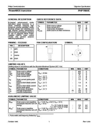
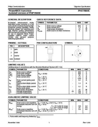
Philips Semiconductors Objective Specification PowerMOS transistor PHP1N60E GENERAL DESCRIPTION QUICK REFERENCE DATA N-channel enhancement mode SYMBOL PARAMETER MAX. UNIT field-effect power transistor in a plastic envelope featuring high VDS Drain-source voltage 600 V avalanche energy capability, stable ID Drain current (DC) 1.9 A blocking voltage, fast switching and Ptot Total power d
0.11. Size:24K philips
phx1n60e 1.pdf
Philips Semiconductors Objective Specification PowerMOS transistor PHX1N60E Isolated version of PHP1N60E GENERAL DESCRIPTION QUICK REFERENCE DATA N-channel enhancement mode SYMBOL PARAMETER MAX. UNIT field-effect power transistor in a full pack, plastic envelope featuring high VDS Drain-source voltage 600 V avalanche energy capability, stable ID Drain current (DC) 1.3 A blocking volt
0.12. Size:559K fairchild semi
fch041n60e.pdf
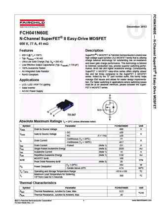
December 2013 FCH041N60E N-Channel SuperFET II Easy-Drive MOSFET 600 V, 77 A, 41 m Features Description 650 V @ TJ = 150 C SuperFET II MOSFET is Fairchild Semiconductor s brand-new high voltage super-junction (SJ) MOSFET family that is utilizing Typ. RDS(on) = 36 m charge balance technology for outstanding low on-resistance Ultra Low Gate Charge (Typ. Qg = 285 nC
0.13. Size:155K vishay
siha21n60ef.pdf

SiHA21N60EF www.vishay.com Vishay Siliconix EF Series Power MOSFET with Fast Body Diode FEATURES D Thin-Lead TO-220 FULLPAK Fast body diode MOSFET using E series technology Reduced trr, Qrr, and IRRM Low figure-of-merit (FOM) Ron x Qg G Low input capacitance (Ciss) Available Increased robustness due to low Qrr Ultra low gate charge (Qg) Avalanche en
0.14. Size:150K vishay
sihh21n60e.pdf

SiHH21N60E www.vishay.com Vishay Siliconix E Series Power MOSFET FEATURES PRODUCT SUMMARY Fully lead (Pb)-free device VDS (V) at TJ max. 650 Low figure-of-merit (FOM) Ron x Qg RDS(on) typ. ( ) at 25 C VGS = 10 V 0.153 Low input capacitance (Ciss) Qg max. (nC) 83 Reduced switching and conduction losses Qgs (nC) 11 Qgd (nC) 20 Ultra low gate charge (Qg) Conf
0.15. Size:152K vishay
sihh11n60e.pdf

SiHH11N60E www.vishay.com Vishay Siliconix E Series Power MOSFET FEATURES PRODUCT SUMMARY Fully lead (Pb)-free device VDS (V) at TJ max. 650 Low figure-of-merit (FOM) Ron x Qg RDS(on) typ. ( ) at 25 C VGS = 10 V 0.295 Low input capacitance (Ciss) Qg max. (nC) 62 Reduced switching and conduction losses Qgs (nC) 7 Qgd (nC) 13 Ultra low gate charge (Qg) Confi
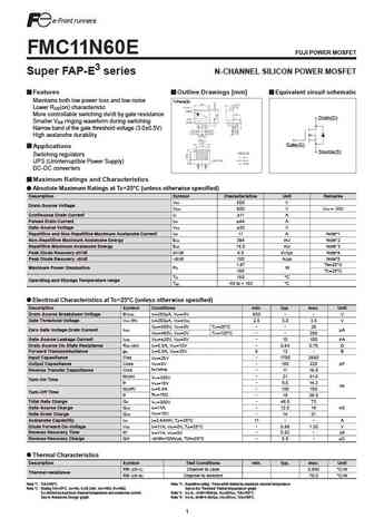
0.16. Size:493K fuji
fmv11n60e.pdf
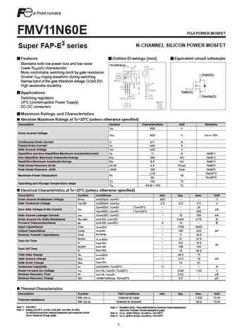
FMV11N60E FUJI POWER MOSFET N-CHANNEL SILICON POWER MOSFET Super FAP-E3 series Features Outline Drawings [mm] Equivalent circuit schematic Maintains both low power loss and low noise TO-220F(SLS) Lower R (on) characteristic DS More controllable switching dv/dt by gate resistance Drain(D) Smaller V ringing waveform during switching GS Narrow band of the gate threshold voltage (3.0 0
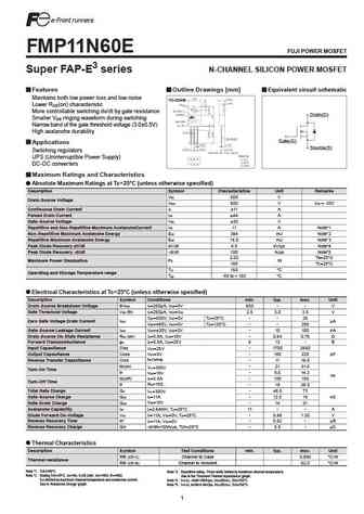
0.17. Size:570K fuji
fmi11n60e.pdf
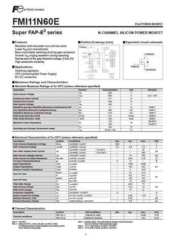
FMI11N60E FUJI POWER MOSFET Super FAP-E3 series N-CHANNEL SILICON POWER MOSFET Features Outline Drawings [mm] Equivalent circuit schematic Maintains both low power loss and low noise T-Pack(L) Lower R (on) characteristic DS More controllable switching dv/dt by gate resistance Drain(D) Smaller V ringing waveform during switching GS Narrow band of the gate threshold voltage (3.0 0.5V)
0.18. Size:567K fuji
fmc11n60e.pdf
FMC11N60E FUJI POWER MOSFET Super FAP-E3 series N-CHANNEL SILICON POWER MOSFET Features Outline Drawings [mm] Equivalent circuit schematic Maintains both low power loss and low noise T-Pack(S) Lower R (on) characteristic DS More controllable switching dv/dt by gate resistance Drain(D) Smaller V ringing waveform during switching GS Narrow band of the gate threshold voltage (3.0 0.5V)
0.19. Size:562K fuji
fmp11n60e.pdf
FMP11N60E FUJI POWER MOSFET Super FAP-E3 series N-CHANNEL SILICON POWER MOSFET Features Outline Drawings [mm] Equivalent circuit schematic Maintains both low power loss and low noise TO-220AB Lower R (on) characteristic DS More controllable switching dv/dt by gate resistance Drain(D) Smaller V ringing waveform during switching GS Narrow band of the gate threshold voltage (3.0 0.5V)
0.20. Size:450K samwin
sw1n60e.pdf
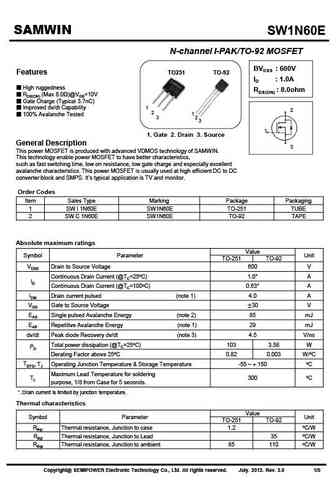
SAMWIN SW1N60E Electrical characteristic ( TC = 25oC unless otherwise specified ) Symbol Parameter Test conditions Min. Typ. Max. Unit Off characteristics BVDSS Drain to source breakdown voltage VGS=0V, ID=250uA 600 V BVDSS Breakdown voltage temperature ID=250uA, referenced to 25oC 0.76 V/oC / TJ coefficient VDS=600V, VGS=0V 1 uA IDSS Drain to source leakage current
0.21. Size:201K inchange semiconductor
fmv11n60e.pdf
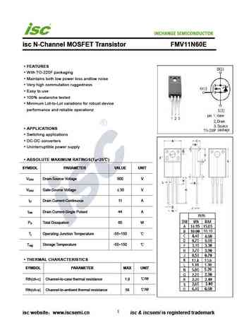
INCHANGE Semiconductor isc N-Channel MOSFET Transistor FMV11N60E FEATURES With TO-220F packaging Maintains both low power loss andlow noise Very high commutation ruggedness Easy to use 100% avalanche tested Minimum Lot-to-Lot variations for robust device performance and reliable operationz APPLICATIONS Switching applications DC-DC converters Uninterruptible po
Otros transistores... 13N60AF
, 16N60A
, 16N60AF
, 16N60B
, 19MT050XFAPBF
, 1HN04CH
, 1HP04CH
, 1N60AF
, IRFZ46N
, 1N60F
, 1N60G
, 20N50B
, 20N60A
, 24N50A
, 24N50B
, 24N50C
, 2MI50S-050
.
History: WMLL099N20HG2
| RCJ050N25
| IXFA102N15T
| MDP18N50TH
