TK12A50D5 MOSFET Equivalente. Reemplazo. Hoja de especificaciones. Principales características
Número de Parte: TK12A50D5
Tipo de FET: MOSFET
Polaridad de transistor: N
ESPECIFICACIONES MÁXIMAS
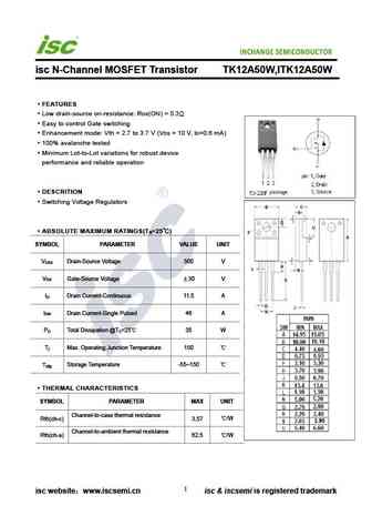
Pdⓘ - Máxima disipación de potencia: 45 W
|Vds|ⓘ - Voltaje máximo drenador-fuente: 500 V
|Vgs|ⓘ - Voltaje máximo fuente-puerta: 30 V
|Id|ⓘ - Corriente continua de drenaje: 12 A
Tjⓘ - Temperatura máxima de unión: 150 °C
CARACTERÍSTICAS ELÉCTRICAS
trⓘ - Tiempo de subida: 25 nS
Cossⓘ - Capacitancia de salida: 160 pF
RDSonⓘ - Resistencia estado encendido drenaje a fuente: 0.73 Ohm
Encapsulados: TO-220F
Búsqueda de reemplazo de TK12A50D5 MOSFET
- Selecciónⓘ de transistores por parámetros
TK12A50D5 datasheet
tk12a50d5.pdf
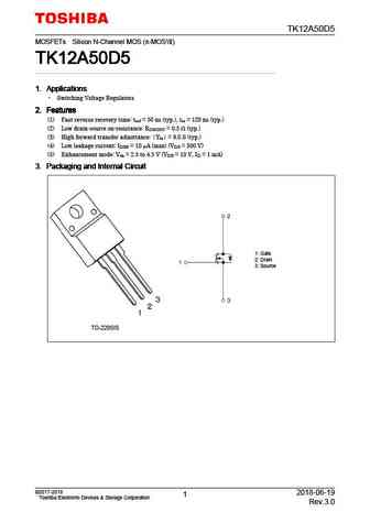
TK12A50D5 MOSFETs Silicon N-Channel MOS ( -MOS ) TK12A50D5 TK12A50D5 TK12A50D5 TK12A50D5 1. Applications 1. Applications 1. Applications 1. Applications Switching Voltage Regulators 2. Features 2. Features 2. Features 2. Features (1) Fast reverse recovery time trrf = 50 ns (typ.), trr = 120 ns (typ.) (2) Low drain-source on-resistance RDS(ON) = 0.5 (typ.) (3) High
tk12a50d5.pdf
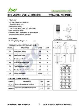
INCHANGE Semiconductor iscN-Channel MOSFET Transistor TK12A50D5 ITK12A50D5 FEATURES Low drain-source on-resistance RDS(ON) = 0.5 (typ.) Enhancement mode Vth = 2.5 to 4.5V (VDS = 10 V, ID=1.0mA) 100% avalanche tested Minimum Lot-to-Lot variations for robust device performance and reliable operation DESCRITION Switching Voltage Regulators ABSOLUTE MAXIMUM RATING
tk12a50d.pdf
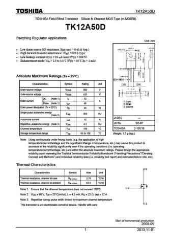
TK12A50D TOSHIBA Field Effect Transistor Silicon N Channel MOS Type ( -MOS ) TK12A50D Switching Regulator Applications Unit mm Low drain-source ON-resistance RDS (ON) = 0.45 (typ.) High forward transfer admittance Yfs = 6.0 S (typ.) Low leakage current IDSS = 10 A (max) (VDS = 500 V) Enhancement mode Vth = 2.0 to 4.0 V (VDS = 10 V, ID = 1 mA) Abs
tk12a50w.pdf
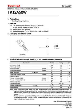
TK12A50W MOSFETs Silicon N-Channel MOS (DTMOS ) TK12A50W TK12A50W TK12A50W TK12A50W 1. Applications 1. Applications 1. Applications 1. Applications Switching Voltage Regulators 2. Features 2. Features 2. Features 2. Features (1) Low drain-source on-resistance RDS(ON) = 0.265 (typ.) by used to Super Junction Structure DTMOS (2) Easy to control Gate switching (3) E
Otros transistores... IRL40B212 , IRL40B215 , IRL60B216 , IRL8114 , TK10A50W , TK10A60D5 , TK10A80W , TK10E80W , IRFZ44 , TK12A50W , TK12A80W , TK17A65W , TK17A65W5 , TK17E80W , TK19A50W , TK22A65X5 , TK290A60Y .
🌐 : EN ES РУ

Liste
Recientemente añadidas las descripciónes de los transistores:
MOSFET: ASU70R600E | ASU65R850E | ASU65R550E | ASU65R350E | ASR65R120EFD | ASR65R046EFD | ASQ65R046EFD | ASM65R280E | ASM60R330E | ASE70R950E | ASD80R750E | ASD70R950E | ASD70R600E | ASD70R380E | ASD65R850E | ASD65R550E
Popular searches
2sc1845 | p60nf06 | 2sa1837 | ksc1845 transistor | irf630 datasheet | mpsa13 equivalent | c5198 | 2sc1969 transistor