AS2301 MOSFET Equivalente. Reemplazo. Hoja de especificaciones. Principales características
Número de Parte: AS2301
Tipo de FET: MOSFET
Polaridad de transistor: P
ESPECIFICACIONES MÁXIMAS
Pdⓘ - Máxima
disipación de potencia: 0.9 W
|Vds|ⓘ - Voltaje máximo drenador-fuente: 20 V
|Vgs|ⓘ - Voltaje máximo fuente-puerta: 10 V
|Id|ⓘ - Corriente continua
de drenaje: 2.8 A
Tjⓘ - Temperatura máxima de unión: 150 °C
CARACTERÍSTICAS ELÉCTRICAS
tonⓘ - Tiempo de encendido: 8 nS
Cossⓘ - Capacitancia de salida: 120 pF
RDSonⓘ - Resistencia estado encendido drenaje a fuente: 0.1 Ohm
Encapsulados: SOT23
Búsqueda de reemplazo de AS2301 MOSFET
- Selecciónⓘ de transistores por parámetros
AS2301 datasheet
..1. Size:1796K anbon
as2301.pdf 
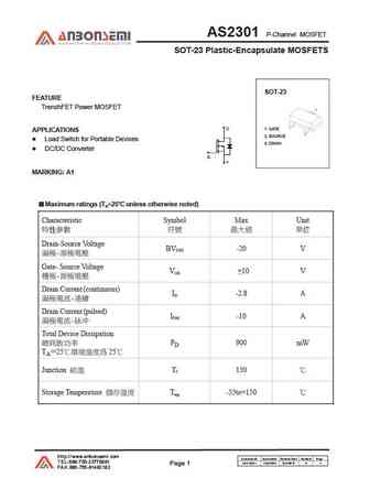
AS2301 P-Channel MOSFET SOT-23 Plastic-Encapsulate MOSFETS SOT-23 FEATURE TrenchFET Power MOSFET 1. GATE APPLICATIONS 2. SOURCE Load Switch for Portable Devices 3. DRAIN DC/DC Converter MARKING A1 Maximum ratings (Ta=25 unless otherwise noted) Characteristic Symbol Max Unit Drain-Source Voltage BVDSS -20 V -
..4. Size:419K fms
as2301.pdf
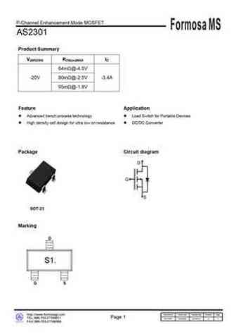
P-Channel Enhancement Mode MOSFET Formosa MS AS2301 Product Summary V(BR)DSS RDS(on)MAX ID 64m @-4.5V -20V 80m @-2.5V -3.4A 95m @-1.8V Feature Application Advanced trench process technology Load Switch for Portable Devices High density cell design for ultra low on-resistance DC/DC Converter Package Circuit diagram SOT-23 Marking S1. Document ID http //www.form
9.1. Size:1783K anbon
as2306.pdf
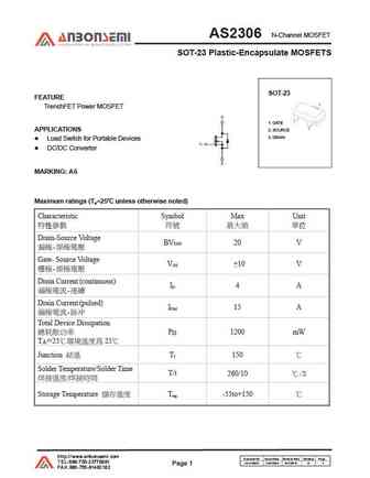
AS2306 N-Channel MOSFET SOT-23 Plastic-Encapsulate MOSFETS SOT-23 FEATURE TrenchFET Power MOSFET 1. GATE APPLICATIONS 2. SOURCE 3. DRAIN Load Switch for Portable Devices DC/DC Converter MARKING A6 Maximum ratings (Ta=25 unless otherwise noted) Characteristic Symbol Max Unit Drain-Source Voltage BV 20 V DSS -
9.2. Size:1817K anbon
as2302.pdf
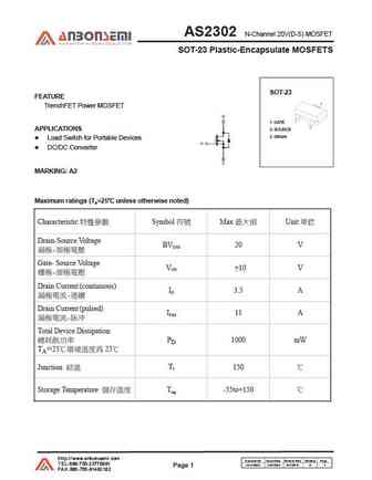
AS2302 N-Channel 20V(D-S) MOSFET SOT-23 Plastic-Encapsulate MOSFETS SOT-23 FEATURE TrenchFET Power MOSFET 1. GATE APPLICATIONS 2. SOURCE 3. DRAIN Load Switch for Portable Devices DC/DC Converter MARKING A2 Maximum ratings (Ta=25 unless otherwise noted) Characteristic Symbol Max Unit Drain-Source Voltage BVDSS 20 V -
9.3. Size:2103K anbon
as2304.pdf
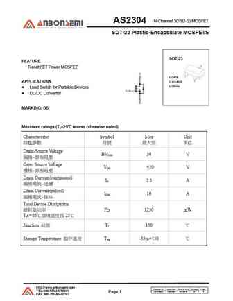
N-Channel 30V(D-S) MOSFET AS2304 SOT-23 Plastic-Encapsulate MOSFETS Dimensions In Millimeters Dimensions In Inches Symbol Min Max Min Max A 0.900 1.150 0.035 0.045 A1 0.000 0.100 0.000 0.004 A2 0.900 1.050 0.035 0.041 b 0.300 0.500 0.012 0.020 c 0.080 0.150 0.003 0.006 D 2.800 3.000 0.110 0.118 E 1.200 1.400 0.047 0.055 E1 2.250 2.550 0.089 0
9.4. Size:2210K anbon
as2308.pdf
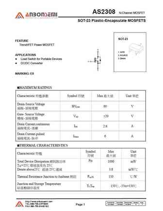
AS2308 N-Channel MOSFET SOT-23 Plastic-Encapsulate MOSFETS Dimensions In Millimeters Dimensions In Inches Symbol Min Max Min Max A 0.900 1.150 0.035 0.045 A1 0.000 0.100 0.000 0.004 A2 0.900 1.050 0.035 0.041 b 0.300 0.500 0.012 0.020 c 0.080 0.150 0.003 0.006 D 2.800 3.000 0.110 0.118 E 1.200 1.400 0.047 0.055 E1 2.250 2.550 0.089 0.100 e 0.9
9.5. Size:1837K anbon
as2305.pdf
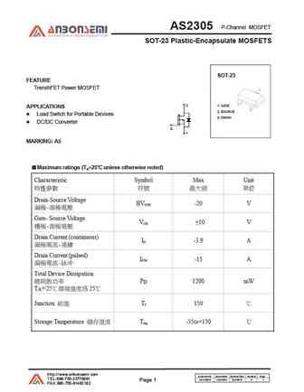
P-Channel MOSFET AS2305 SOT-23 Plastic-Encapsulate MOSFETS SOT-23 FEATURE TrenchFET Power MOSFET 1. GATE APPLICATIONS 2. SOURCE Load Switch for Portable Devices 3. DRAIN DC/DC Converter MARKING A5 Maximum ratings (Ta=25 unless otherwise noted) Characteristic Symbol Max Unit Drain-Source Voltage BV -20 V DSS -
9.6. Size:761K anbon
as2309.pdf
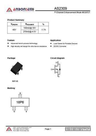
AS2309 P-Channel Enhancement Mode MOSFET Product Summary V(BR)DSS RDS(on)MAX ID 180m @-10V -60V -1.7A 270m @-4.5V Feature Application Advanced trench process technology Load Switch for Portable Devices High density cell design for ultra low on-resistance DC/DC Converter Package Circuit diagram SOT-23 Marking 18P6 Document ID Issued Date Revised Date Revision Page
9.7. Size:678K anbon
as2300.pdf
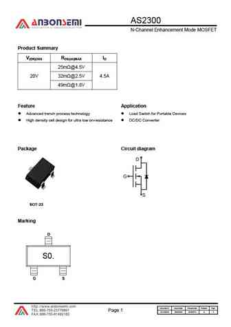
AS2300 N-Channel Enhancement Mode MOSFET Product Summary V(BR)DSS RDS(on)MAX ID 25m @4.5V 20V 32m @2.5V 4.5A 49m @1.8V Feature Application Advanced trench process technology Load Switch for Portable Devices High density cell design for ultra low on-resistance DC/DC Converter Package Circuit diagram SOT-23 Marking S0. Document ID Issued Date Revised Date Revision
9.8. Size:2062K anbon
as2303.pdf
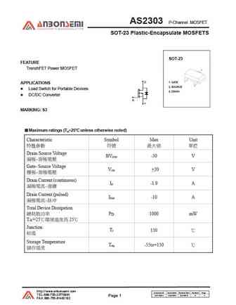
AS2303 P-Channel MOSFET SOT-23 Plastic-Encapsulate MOSFETS Dimensions In Millimeters Dimensions In Inches Symbol Min Max Min Max A 0.900 1.150 0.035 0.045 A1 0.000 0.100 0.000 0.004 A2 0.900 1.050 0.035 0.041 b 0.300 0.500 0.012 0.020 c 0.080 0.150 0.003 0.006 D 2.800 3.000 0.110 0.118 E 1.200 1.400 0.047 0.055 E1 2.250 2.550 0.089 0.100 e 0.9
9.9. Size:1915K anbon
as2307.pdf
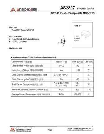
P-Channel MOSFET AS2307 SOT-23 Plastic-Encapsulate MOSFETS SOT-23 FEATURE TrenchFET Power MOSFET 1. GATE APPLICATIONS 2. SOURCE Load Switch for Portable Devices 3. DRAIN DC/DC Converter MARKING B 1 1 Maximum ratings (Ta=25 unless otherwise noted) Characteristic Symbol Max Unit Drain-Source Voltage - BV
9.10. Size:400K fms
as2302.pdf
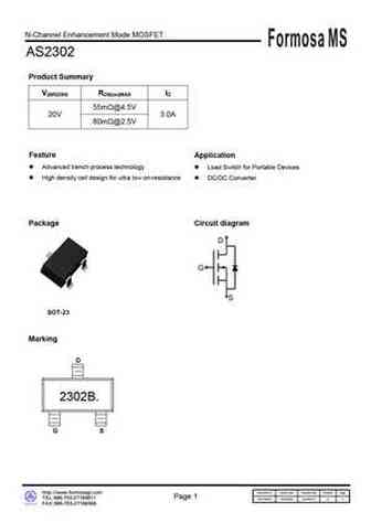
N-Channel Enhancement Mode MOSFET Formosa MS AS2302 Product Summary V(BR)DSS RDS(on)MAX ID 55m @4.5V 20V 3.0A 80m @2.5V Feature Application Advanced trench process technology Load Switch for Portable Devices High density cell design for ultra low on-resistance DC/DC Converter Package Circuit diagram SOT-23 Marking 2302B. Document ID http //www.formosagr.com Doc
Otros transistores... AD50N06S
, AD90N03S
, AO6385
, AS0130KA
, AS2003M
, AS2101W
, AS2102W
, AS2300
, IRF730
, AS2302
, AS2303
, AS2304
, AS2305
, AS2307
, BM2300
, BM3402
, BM3407A
.
History: 2SK3922-01
| S2N7002K
| NCE60R360F
| SGM3055
| HCFL65R380
| BSC13DN30NSFD


