100N10NF MOSFET Equivalente. Reemplazo. Hoja de especificaciones. Principales características
Número de Parte: 100N10NF
Tipo de FET: MOSFET
Polaridad de transistor: N
ESPECIFICACIONES MÁXIMAS
Pdⓘ - Máxima
disipación de potencia: 50 W
|Vds|ⓘ - Voltaje máximo drenador-fuente: 100 V
|Vgs|ⓘ - Voltaje máximo fuente-puerta: 20 V
|Id|ⓘ - Corriente continua
de drenaje: 100 A
Tjⓘ - Temperatura máxima de unión: 150 °C
CARACTERÍSTICAS ELÉCTRICAS
trⓘ - Tiempo
de subida: 3 nS
Cossⓘ - Capacitancia de salida: 172 pF
RDSonⓘ - Resistencia estado encendido drenaje a fuente: 0.0084 Ohm
Encapsulados: TO220F
Búsqueda de reemplazo de 100N10NF MOSFET
- Selecciónⓘ de transistores por parámetros
100N10NF datasheet
..1. Size:446K chongqing pingwei
100n10nf.pdf 
100N10NF 100 Amps,100 Volts N-CHANNEL Power MOSFET FEATURE TO-220NF 100A,100V,R =8.4m V =10V/20A DS(ON)MAX GS Low gate charge Low C iss Fast switching 100% avalanche tested Improved dv/dt capability Absolute Maximum Ratings(T =25 ,unless otherwise noted) C Parameter Symbol UNIT 100N10NF Drain-Source Voltage V 100 DSS V Gate-Source Voltage V 20 GS
8.1. Size:185K motorola
mty100n10e.pdf
MOTOROLA Order this document SEMICONDUCTOR TECHNICAL DATA by MTY100N10E/D Designer's Data Sheet MTY100N10E TMOS E-FET. Motorola Preferred Device Power Field Effect Transistor N Channel Enhancement Mode Silicon Gate TMOS POWER FET This advanced TMOS power FET is designed to withstand high 100 AMPERES energy in the avalanche and commutation modes. This new energy 100 VOLTS
8.2. Size:216K motorola
mgy100n10e.pdf

MOTOROLA Order this document SEMICONDUCTOR TECHNICAL DATA by MTY100N10E/D Designer's Data Sheet MTY100N10E TMOS E-FET. Motorola Preferred Device Power Field Effect Transistor N Channel Enhancement Mode Silicon Gate TMOS POWER FET This advanced TMOS power FET is designed to withstand high 100 AMPERES energy in the avalanche and commutation modes. This new energy 100 VOLTS
8.3. Size:1657K st
stb100n10f7 std100n10f7 stf100n10f7 stf100n10f7 stp100n10f7.pdf
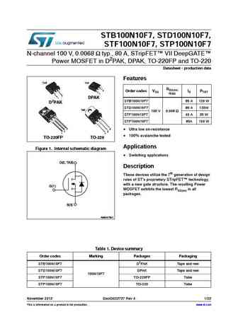
STB100N10F7, STD100N10F7, STF100N10F7, STP100N10F7 N-channel 100 V, 0.0068 typ., 80 A, STripFET VII DeepGATE Power MOSFET in D2PAK, DPAK, TO-220FP and TO-220 Datasheet - production data Features TAB TAB RDS(on) 3 Order codes VDS max ID PTOT 1 3 1 DPAK STB100N10F7 80 A 120 W D2PAK STD100N10F7 80 A 120W TAB 100 V 0.008 STF100N10F7 45 A 30 W STP100N10F7 80A 150 W
8.4. Size:628K st
strh100n10.pdf
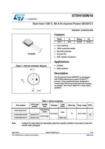
STRH100N10 Rad-Hard 100 V, 48 A N-channel Power MOSFET Datasheet - production data Features VBDSS ID RDS(on) Qg 100 V 48 A 30 m 135 nC Fast switching 100% avalanche tested 3 2 Hermetic package 1 TO-254AA 70 krad TID SEE radiation hardened Applications Satellite Figure 1. Internal schematic diagram High reliability D(1) Description This N-chan
8.5. Size:1396K st
stl100n10f7.pdf
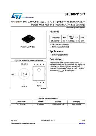
STL100N10F7 N-channel 100 V, 0.0062 typ., 19 A, STripFET VII DeepGATE Power MOSFET in a PowerFLAT 5x6 package Datasheet - production data Features RDS(on) Order code VDSS max ID PTOT 1 STL100N10F7 100 V 0.0073 19 A 5 W 2 3 4 Ultra low on-resistance PowerFLAT 5x6 100% avalanche tested Applications Switching applications Description Figure 1. Int
8.6. Size:648K st
stb100n10f7 std100n10f7 stf100n10f7 sti100n10f7 stp100n10f7.pdf
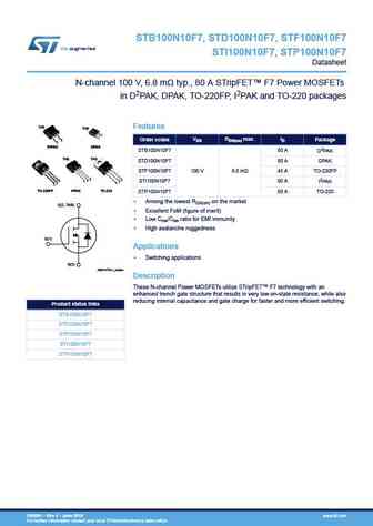
STB100N10F7, STD100N10F7, STF100N10F7 STI100N10F7, STP100N10F7 Datasheet N-channel 100 V, 6.8 m typ., 80 A STripFET F7 Power MOSFETs in D2PAK, DPAK, TO-220FP, I2PAK and TO-220 packages TAB TAB Features 2 3 1 VDS RDS(on) max. ID Order codes Package 3 1 D2PAK DPAK STB100N10F7 80 A D2PAK TAB TAB STD100N10F7 80 A DPAK STF100N10F7 100 V 8.0 m 45 A TO-220FP 3 3 2 3 1 2
8.7. Size:703K fairchild semi
fdp100n10.pdf
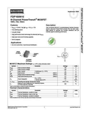
September 2009 FDP100N10 tm N-Channel PowerTrench MOSFET 100V, 75A, 10m Features Description RDS(on) = 8.2m ( Typ.)@ VGS = 10V, ID = 75A This N-Channel MOSFET is producedusing Fairchild Semicon- ductor s advanced PowerTrench process that has been espe- Fast switching speed cially tailored to minimize the on-state resistance and yet maintain superior switching perfo
8.8. Size:1374K rohm
rsd100n10fra.pdf
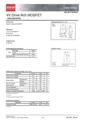
Data Sheet AEC-Q101 Qualified 4V Drive Nch MOSFET RSD100N10 RSD100N10FRA Structure Dimensions (Unit mm) Silicon N-channel MOSFET CPT3 6.5 (SC-63) 5.1 2.3 0.5 Features 1) Low on-resistance. 2) 4V drive. 0.75 3) High power package. 0.65 0.9 2.3 (1) (2) (3) 2.3 0.5 1.0 Application Switching Packaging specifications Inner circuit Packag
8.9. Size:1155K rohm
rsd100n10.pdf
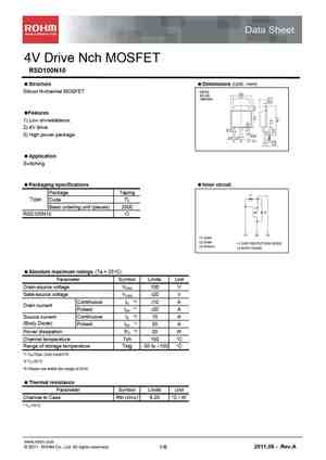
Data Sheet 4V Drive Nch MOSFET RSD100N10 Structure Dimensions (Unit mm) Silicon N-channel MOSFET CPT3 6.5 (SC-63) 5.1 2.3 0.5 Features 1) Low on-resistance. 2) 4V drive. 0.75 3) High power package. 0.65 0.9 2.3 (1) (2) (3) 2.3 0.5 1.0 Application Switching Packaging specifications Inner circuit Package Taping 1 Type Code TL Bas
8.10. Size:168K vishay
sqm100n10-10.pdf
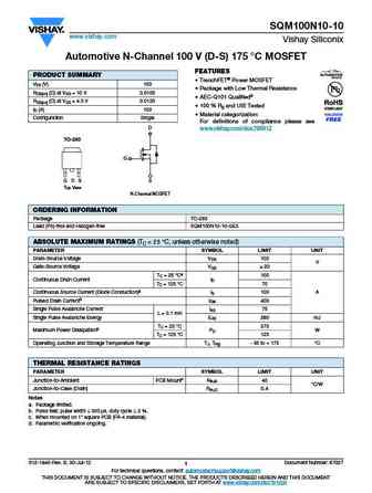
SQM100N10-10 www.vishay.com Vishay Siliconix Automotive N-Channel 100 V (D-S) 175 C MOSFET FEATURES PRODUCT SUMMARY TrenchFET Power MOSFET VDS (V) 100 Package with Low Thermal Resistance RDS(on) ( ) at VGS = 10 V 0.0105 AEC-Q101 Qualifiedd RDS(on) ( ) at VGS = 4.5 V 0.0120 100 % Rg and UIS Tested ID (A) 100 Material categorization Configuration Sin
8.11. Size:186K infineon
ipb100n10s3-05 ipi100n10s3-05 ipp100n10s3-05.pdf
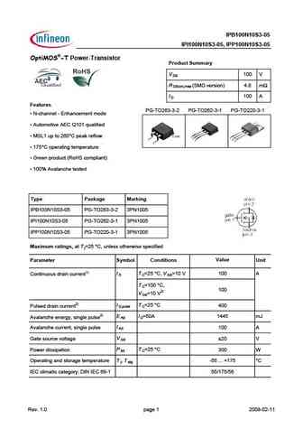
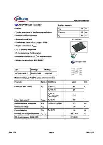
IPB100N10S3-05 IPI100N10S3-05, IPP100N10S3-05 OptiMOS -T Power-Transistor Product Summary V 100 V DS R (SMD version) 4.8 m DS(on),max I 100 A D Features PG-TO263-3-2 PG-TO262-3-1 PG-TO220-3-1 N-channel - Enhancement mode Automotive AEC Q101 qualified MSL1 up to 260 C peak reflow 175 C operating temperature Green product (RoHS compliant) 100% Aval
8.13. Size:191K infineon
ipi100n10s3-05 ipp100n10s3-05 ipb100n10s3-05.pdf
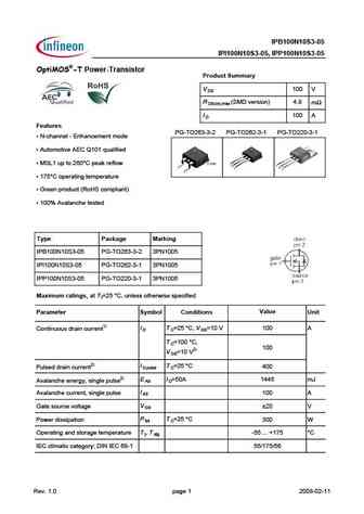
IPB100N10S3-05 IPI100N10S3-05, IPP100N10S3-05 OptiMOS -T Power-Transistor Product Summary V 100 V DS R (SMD version) 4.8 m DS(on),max I 100 A D Features PG-TO263-3-2 PG-TO262-3-1 PG-TO220-3-1 N-channel - Enhancement mode Automotive AEC Q101 qualified MSL1 up to 260 C peak reflow 175 C operating temperature Green product (RoHS compliant) 100% Aval
8.14. Size:563K infineon
iauc100n10s5l040.pdf
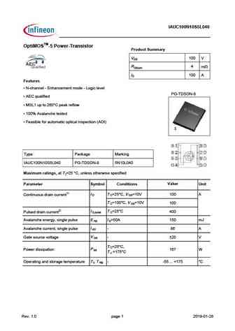
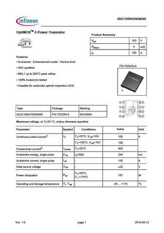
IAUC100N10S5L040 OptiMOSTM-5 Power-Transistor Product Summary VDS 100 V RDS(on) 4 mW ID 100 A Features N-channel - Enhancement mode - Logic level PG-TDSON-8 AEC qualified MSL1 up to 260 C peak reflow 100% Avalanche tested Feasible for automatic optical inspection (AOI) 1 Type Package Marking IAUC100N10S5L040 PG-TDSON-8 5N10L040 Maximum ratings, at T =25 C
8.15. Size:99K ixys
ixfn100n10s1-s2-s3.pdf
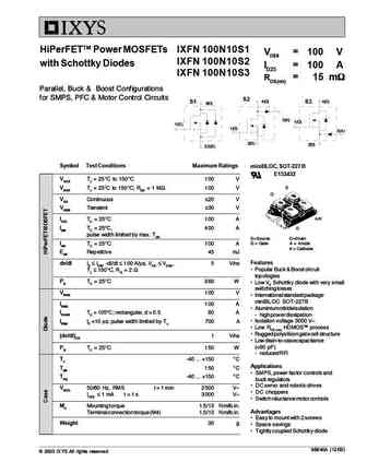
HiPerFETTM Power MOSFETs IXFN 100N10S1 VDSS = 100 V IXFN 100N10S2 with Schottky Diodes ID25 = 100 A IXFN 100N10S3 RDS(on) = 15 m m I=_ =C==_ = =pjmpI=mc =C=j = = S2 QEaF QEaF S1 S3 QEaF PEhF NEdF NEdF NEdF PE^F OEpF OEpF OIPEpF Symbol Test Conditions Maximum Rati
8.16. Size:117K ixys
ixfk100n10 ixfn150n10.pdf
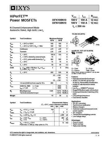
VDSS ID25 RDS(on) HiPerFETTM IXFK100N10 100 V 100 A 12 mW Power MOSFETs IXFN150N10 100 V 150 A 12 mW trr 200 ns N-Channel Enhancement Mode Avalanche Rated, High dv/dt, Low trr TO-264 AA (IXFK) Symbol Test Conditions Maximum Ratings IXFK IXFN VDSS TJ = 25 C to 150 C 100 100 V G (TAB) VDGR TJ = 25 C to 150 C; RGS = 1 MW 100 100 V D S VGS Continuous 20 20 V miniBLOC, SOT
8.17. Size:613K onsemi
ndpl100n10b ndpl100n10bg.pdf
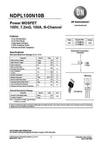
NDPL100N10B Power MOSFET www.onsemi.com 100V, 7.2m , 100A, N-Channel Features Low On-Resistance VDSS RDS(on) Max ID Max Low Gate Charge 7.2 m @15V High Speed Switching 100V 100A 8.7 m @10V 100% Avalanche Tested Pb-Free and RoHS Compliance Electrical Connection Specifications N-Channel Absolute Maximum Ratings at Ta = 25 C 2 Parameter Sy
8.18. Size:157K onsemi
nty100n10.pdf
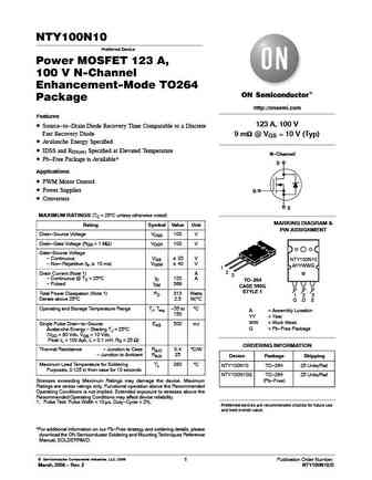
NTY100N10 Preferred Device Power MOSFET 123 A, 100 V N-Channel Enhancement-Mode TO264 Package http //onsemi.com Features 123 A, 100 V Source-to-Drain Diode Recovery Time Comparable to a Discrete Fast Recovery Diode 9 mW @ VGS = 10 V (Typ) Avalanche Energy Specified IDSS and RDS(on) Specified at Elevated Temperature N-Channel Pb-Free Package is Available* D Appl
8.19. Size:616K onsemi
ndba100n10b.pdf
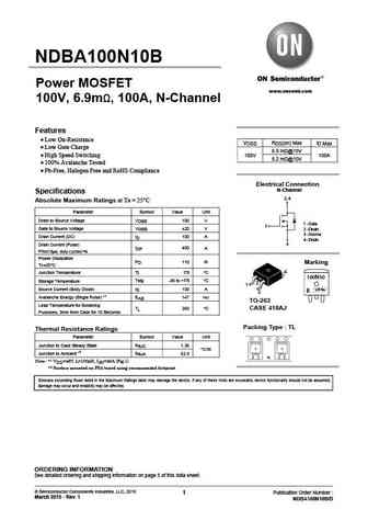
NDBA100N10B Power MOSFET www.onsemi.com 100V, 6.9m , 100A, N-Channel Features Low On-Resistance VDSS RDS(on) Max ID Max Low Gate Charge 6.9 m @15V High Speed Switching 100V 100A 8.2 m @10V 100% Avalanche Tested Pb-Free, Halogen Free and RoHS Compliance Electrical Connection N-Channel Specifications 2, 4 Absolute Maximum Ratings at Ta = 2
8.20. Size:207K onsemi
mty100n10e.pdf
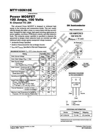
MTY100N10E Preferred Device Power MOSFET 100 Amps, 100 Volts N-Channel TO-264 This advanced Power MOSFET is designed to withstand high energy in the avalanche and commutation modes. This new energy http //onsemi.com efficient design also offers a drain-to-source diode with fast recovery time. Designed for high voltage, high speed switching applications in 100 AMPERES power supplies,
8.21. Size:1622K blue-rocket-elect
brcs100n10shzc.pdf
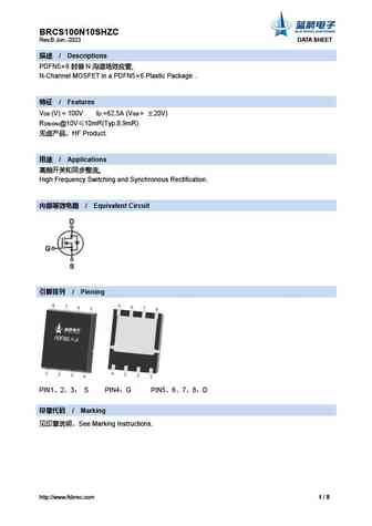
BRCS100N10SHZC Rev.B Jun.-2023 DATA SHEET / Descriptions PDFN5 6 N N-Channel MOSFET in a PDFN5 6 Plastic Package . / Features V (V) = 100V I =62.5A (V = 20V) DS D GS R DS(ON)@10V 10mR(Typ.8.9mR) HF Product. / Applications High Frequency Switching and Synchronous Recti
8.22. Size:293K first silicon
ftk100n10p.pdf
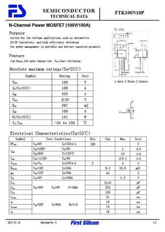
SEMICONDUCTOR FTK100N10P TECHNICAL DATA N-Channel Power MOSFET (100V/100A) Purpose Suited for low voltage applications such as automotive, DC/DC Converters, and high efficiency switching for power management in portable and battery operated products Feature Low RDS(on),low gate charge,low Crss,fast switching. Absolute maximum ratings(Ta=25 ) Symbol Rating Unit 1.Gate 2.Drai
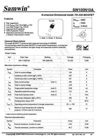
8.27. Size:701K samwin
swp100n10b.pdf
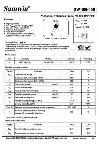
SW100N10B N-channel Enhanced mode TO-220 MOSFET Features BVDSS 100V TO-220 High ruggedness ID 120A Low RDS(ON) (Typ 6.7m )@VGS=10V RDS(ON) 6.7m Low Gate Charge (Typ 106nC) Improved dv/dt Capability 2 100% Avalanche Tested 1 Application Synchronous Rectification, 2 3 Li Battery Protect Board, Inverter 1 1. Gate 2. Drain 3. Source 3 General
8.28. Size:624K samwin
swp100n10a.pdf
SW100N10A N-channel Enhanced mode TO-220 MOSFET Features BVDSS 100V TO-220 High ruggedness ID 100A Low RDS(ON) (Typ 5.9m )@VGS=10V RDS(ON) 5.9m Low Gate Charge (Typ 127nC) Improved dv/dt Capability 2 100% Avalanche Tested Application Synchronous Rectification, 1 2 Li Battery Protect Board, Inverter 3 1 1. Gate 2. Drain 3. S
8.29. Size:599K way-on
wmk100n10ts.pdf
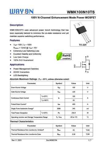
WMK100N10TS 100V N-Channel Enhancement Mode Power MOSFET Description WMK100N10TS uses advanced power trench technology that has been especially tailored to minimize the on-state resistance and yet maintain superior switching performance. Features S D G V = 100V, I = 100A DS D TO-220 R
8.30. Size:360K dacosemi
damia1100n100.pdf

DAMIA1100N100 DACO SEMICONDUCTOR CO., LTD. N-Channel Enhancement Mode MOSFET SOT-227H Preliminary Features S D VDSS = 100V RDS(ON)
8.31. Size:203K inchange semiconductor
stb100n10f7.pdf
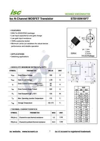
INCHANGE Semiconductor Isc N-Channel MOSFET Transistor STB100N10F7 FEATURES With To-263(D2PAK) package Low input capacitance and gate charge Low gate input resistance 100% avalanche tested Minimum Lot-to-Lot variations for robust device performance and reliable operation APPLICATIONS Switching applications ABSOLUTE MAXIMUM RATINGS(T =25 ) a SYMBOL PARAMETER VALU
8.32. Size:243K inchange semiconductor
std100n10f7.pdf
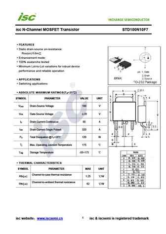
isc N-Channel MOSFET Transistor STD100N10F7 FEATURES Static drain-source on-resistance RDS(on) 8m Enhancement mode 100% avalanche tested Minimum Lot-to-Lot variations for robust device performance and reliable operation APPLICATIONS Switching applications ABSOLUTE MAXIMUM RATINGS(T =25 ) a SYMBOL PARAMETER VALUE UNIT V Drain-Source Voltage 100 V DSS V Gat
8.33. Size:205K inchange semiconductor
stp100n10f7.pdf
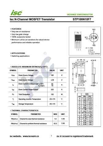
INCHANGE Semiconductor Isc N-Channel MOSFET Transistor STP100N10F7 FEATURES Very low on-resistance Very low gate charge 100% avalanche tested Minimum Lot-to-Lot variations for robust device performance and reliable operation APPLICATIONS Switching applications ABSOLUTE MAXIMUM RATINGS(T =25 ) a SYMBOL PARAMETER VALUE UNIT V Drain-Source Voltage 100 V DSS V Gate-
8.34. Size:206K inchange semiconductor
fdp100n10.pdf
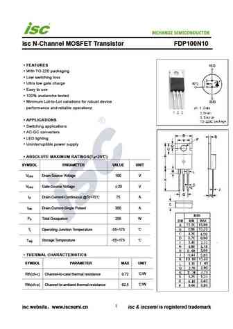
INCHANGE Semiconductor isc N-Channel MOSFET Transistor FDP100N10 FEATURES With TO-220 packaging Low switching loss Ultra low gate charge Easy to use 100% avalanche tested Minimum Lot-to-Lot variations for robust device performance and reliable operationz APPLICATIONS Switching applications AC-DC converters LED lighting Uninterruptible power supply ABSOLU
8.35. Size:1412K cn apm
apg100n10d.pdf
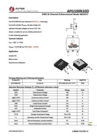
APG100N10D 100V N-Channel Enhancement Mode MOSFET Description The APG100N10D uses advanced APM-SGT technology to provide excellent R , low gate charge and DS(ON) operation with gate voltages as low as 4.5V. This device is suitable for use as a Battery protection or in other Switching application. General Features V = 100V I =100A DS D R
Otros transistores... AK7N60S
, AG7N60S
, AU8N60S
, AD8N60S
, AT8N60S
, AF8N60S
, AK8N60S
, AG8N60S
, IRFZ24N
, 10N50TF
, 11N65GS
, 11N65TFS
, 12N60B
, 12N60H
, 12N65
, 12N65F
, 12N65B
.