25N06G MOSFET Equivalente. Reemplazo. Hoja de especificaciones. Principales características
Número de Parte: 25N06G
Tipo de FET: MOSFET
Polaridad de transistor: N
ESPECIFICACIONES MÁXIMAS
Pdⓘ - Máxima disipación de potencia: 50 W
|Vds|ⓘ - Voltaje máximo drenador-fuente: 60 V
|Vgs|ⓘ - Voltaje máximo fuente-puerta: 20 V
|Id|ⓘ - Corriente continua de drenaje: 25 A
Tjⓘ - Temperatura máxima de unión: 150 °C
CARACTERÍSTICAS ELÉCTRICAS
trⓘ - Tiempo de subida: 19 nS
Cossⓘ - Capacitancia de salida: 117 pF
RDSonⓘ - Resistencia estado encendido drenaje a fuente: 0.036 Ohm
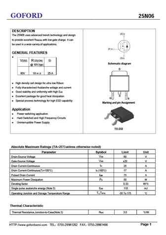
Encapsulados: TO252
Búsqueda de reemplazo de 25N06G MOSFET
- Selecciónⓘ de transistores por parámetros
25N06G datasheet
25n06g.pdf
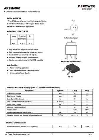
25N06D&25N06G POWER MOSFET Featutes 25A,60V,R =0.036 @V =10V/12.5A DS(ON)MAX GS Low gate charge Low C iss Fast switching 100% avalanche tested Improved dv/dt capability TO-251(IPAK) TO-252(DPAK) 25N06D 25N06G Absolute Maximum Ratings(T =25 ,unless otherwise noted) C Parameter Symbol 25N06D&25N06G UNIT Drain-Source Voltage V 60 DSS V Gate-Source Vol
hyg025n06ls1c2.pdf
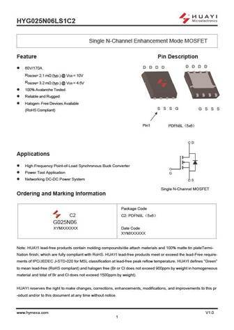
HYG025N06LS1C2 Single N-Channel Enhancement Mode MOSFET Feature Pin Description D D D D D D D D 60V/170A RDS(ON)= 2.1 m (typ.) @ VGS = 10V RDS(ON)= 3.2 m (typ.) @ VGS = 4.5V 100% Avalanche Tested Reliable and Rugged Halogen- Free Devices Available S S S G G S S S (RoHS Compliant) Pin1 PDFN8L 5x6 Applications High Frequency Point-of-Load Synchronous B
php125n06lt 4.pdf
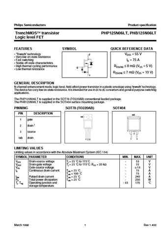
Philips Semiconductors Product specification TrenchMOS transistor PHP125N06LT, PHB125N06LT Logic level FET FEATURES SYMBOL QUICK REFERENCE DATA Trench technology VDSS = 55 V d Very low on-state resistance Fast switching ID = 75 A Stable off-state characteristics High thermal cycling performance RDS(ON) 8 m (VGS = 5 V) g Low thermal resistance
php125n06t 1.pdf
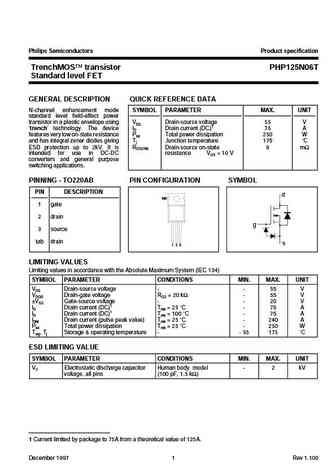
Philips Semiconductors Product specification TrenchMOS transistor PHP125N06T Standard level FET GENERAL DESCRIPTION QUICK REFERENCE DATA N-channel enhancement mode SYMBOL PARAMETER MAX. UNIT standard level field-effect power transistor in a plastic envelope using VDS Drain-source voltage 55 V trench technology. The device ID Drain current (DC)1 75 A features very low on-state
phb125n06l.pdf

Philips Semiconductors Product specification TrenchMOS transistor PHB125N06LT Logic level FET GENERAL DESCRIPTION QUICK REFERENCE DATA N-channel enhancement mode logic SYMBOL PARAMETER MAX. UNIT level field-effect power transistor in a plastic envelope suitable for surface VDS Drain-source voltage 55 V mounting Using trench technology ID Drain current (DC)1 75 A the device fe
phb125n06t 1.pdf

Philips Semiconductors Product specification TrenchMOS transistor PHB125N06T Standard level FET GENERAL DESCRIPTION QUICK REFERENCE DATA N-channel enhancement mode SYMBOL PARAMETER MAX. UNIT standard level field-effect power transistor in a plastic envelope VDS Drain-source voltage 55 V suitable for surface mounting. Using ID Drain current (DC)1 75 A trench technology the dev
stp25n06.pdf
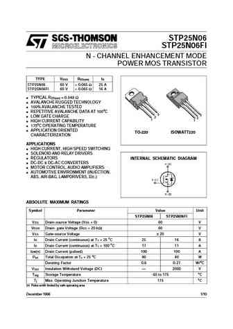
STP25N06 STP25N06FI N - CHANNEL ENHANCEMENT MODE POWER MOS TRANSISTOR TYPE VDSS RDS(on) ID STP25N06 60 V
fdp025n06.pdf
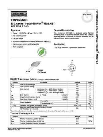
July 2008 FDP025N06 tm N-Channel PowerTrench MOSFET 60V, 265A, 2.5m Features General Description RDS(on) = 1.9m ( Typ.) @ VGS = 10V, ID = 75A This N-Channel MOSFET is produced using Fairchild Semiconductor s advanced PowerTrench process that has been Fast switching speed especially tailored to minimize the on-state resistance and yet maintain superior switching p
fdi025n06.pdf
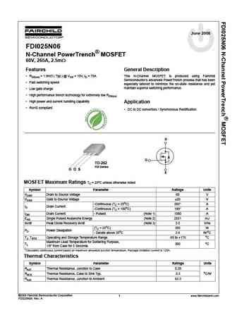
June 2008 FDI025N06 tm N-Channel PowerTrench MOSFET 60V, 265A, 2.5m Features General Description RDS(on) = 1.9m ( Typ.) @ VGS = 10V, ID = 75A This N-Channel MOSFET is produced using Fairchild Semiconductor s advanced PowerTrench process that has been Fast switching speed especially tailored to minimize the on-state resistance and yet maintain superior switching p
sqd25n06-22l.pdf
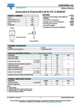
SQD25N06-22L www.vishay.com Vishay Siliconix Automotive N-Channel 60 V (D-S) 175 C MOSFET FEATURES PRODUCT SUMMARY Halogen-free According to IEC 61249-2-21 VDS (V) 60 Definition RDS(on) ( ) at VGS = 10 V 0.022 TrenchFET Power MOSFET RDS(on) ( ) at VGS = 4.5 V 0.033 Package with Low Thermal Resistance ID (A) 25 100 % Rg and UIS Tested Configuration Single
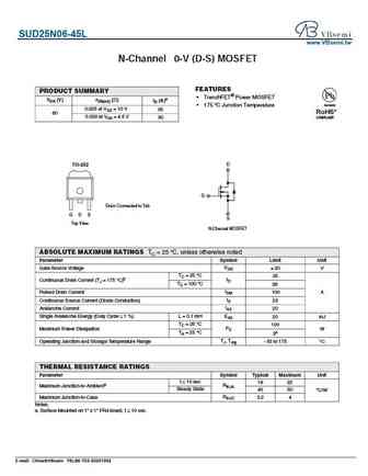
sud25n06-45l.pdf
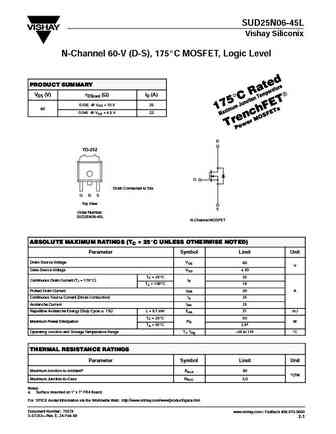
SUD25N06-45L Vishay Siliconix N-Channel 60-V (D-S), 175_C MOSFET, Logic Level PRODUCT SUMMARY VDS (V) rDS(on) (W) ID (A) 0.035 @ VGS = 10 V 25 60 60 0.045 @ VGS = 4.5 V 22 D TO-252 G Drain Connected to Tab G D S Top View S Order Number SUD25N06-45L N-Channel MOSFET ABSOLUTE MAXIMUM RATINGS (TC = 25_C UNLESS OTHERWISE NOTED) Parameter Symbol Limit Unit Drain-Source Voltage
ipd025n06n.pdf
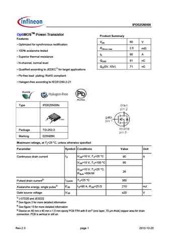
Type IPD025N06N OptiMOSTM Power-Transistor Product Summary Features VDS 60 V Optimized for synchronous rectification RDS(on),max 2.5 mW 100% avalanche tested ID 90 A Superior thermal resistance QOSS 81 nC N-channel, normal level QG(0V..10V) 71 nC Qualified according to JEDEC1) for target applications Pb-free lead plating; RoHS compliant Haloge
ipp25n06s3-25.pdf
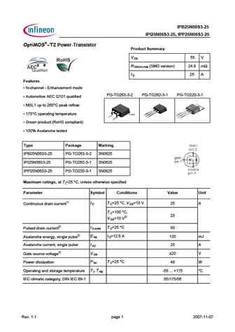
IPB25N06S3-25 IPI25N06S3-25, IPP25N06S3-25 OptiMOS -T2 Power-Transistor Product Summary V 55 V DS R (SMD version) 24.8 m DS(on),max I 25 A D Features N-channel - Enhancement mode PG-TO263-3-2 PG-TO262-3-1 PG-TO220-3-1 Automotive AEC Q101 qualified MSL1 up to 260 C peak reflow 175 C operating temperature Green product (RoHS compliant) 100% Avalanch
ipd25n06s4l-30.pdf
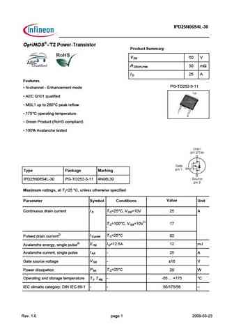
IPD25N06S4L-30 OptiMOS -T2 Power-Transistor Product Summary V 60 V DS R 30 m DS(on),max I 25 A D Features PG-TO252-3-11 N-channel - Enhancement mode AEC Q101 qualified MSL1 up to 260 C peak reflow 175 C operating temperature Green Product (RoHS compliant) 100% Avalanche tested Type Package Marking IPD25N06S4L-30 PG-TO252-3-11 4N06L30 Maximum rat
ipd25n06s2-40.pdf
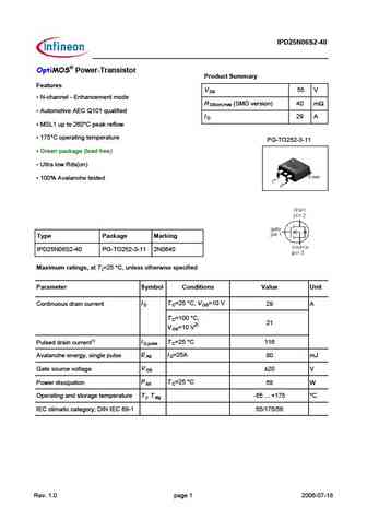
IPD25N06S2-40 OptiMOS Power-Transistor Product Summary Features V 55 V DS N-channel - Enhancement mode R (SMD version) 40 m DS(on),max Automotive AEC Q101 qualified I 29 A D MSL1 up to 260 C peak reflow 175 C operating temperature PG-TO252-3-11 Green package (lead free) Ultra low Rds(on) 100% Avalanche tested Type Package Marking IPD25N06S2
25n06.pdf

UNISONIC TECHNOLOGIES CO., LTD 25N06 Preliminary Power MOSFET 25A, 60V N-CHANNEL POWER MOSFET DESCRIPTION The UTC 25N06 is an N-channel enhancement mode power MOSFET, which provides low gate charge, avalanche rugged technology, and so on. The UTC 25N06 is universally applied in DC-DC & DC-AC converters, motor control, high current, high speed switching, solenoid and relay
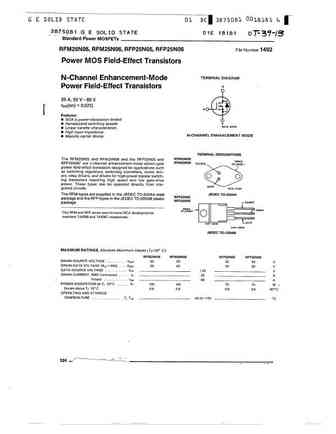
rf1s25n06.pdf
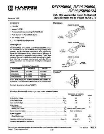
RFP25N06, RF1S25N06, S E M I C O N D U C T O R RF1S25N06SM 25A, 60V, Avalanche Rated N-Channel Enhancement-Mode Power MOSFETs December 1995 Features Packages JEDEC TO-220AB 25A, 60V SOURCE DRAIN GATE rDS(ON) = 0.047 Temperature Compensating PSPICE Model Peak Current vs Pulse Width Curve DRAIN UIS Rating Curve (FLANGE) +175oC Operating Temperature JED
rfp25n06 rf1s25n06sm.pdf
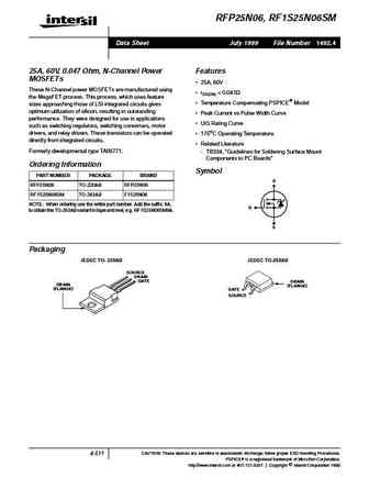
RFP25N06, RF1S25N06SM Data Sheet July 1999 File Number 1492.4 25A, 60V, 0.047 Ohm, N-Channel Power Features MOSFETs 25A, 60V These N-Channel power MOSFETs are manufactured using rDS(ON) = 0.047 the MegaFET process. This process, which uses feature Temperature Compensating PSPICE Model sizes approaching those of LSI integrated circuits gives optimum utilization of sili
cs25n06 b3.pdf
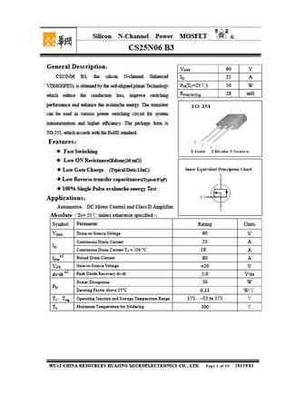
Silicon N-Channel Power MOSFET R CS25N06 B3 General Description VDSS 60 V CS25N06 B3, the silicon N-channel Enhanced ID 25 A PD(TC=25 ) 50 W VDMOSFETs, is obtained by the self-aligned planar Technology RDS(ON)Typ 28 m which reduce the conduction loss, improve switching performance and enhance the avalanche energy. The transistor can be used in various power s
cs25n06 b8.pdf
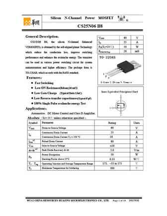
Silicon N-Channel Power MOSFET R CS25N06 B8 General Description VDSS 60 V CS25N06 B8, the silicon N-channel Enhanced ID 25 A PD(TC=25 ) 50 W VDMOSFETs, is obtained by the self-aligned planar Technology RDS(ON)Typ 28 m which reduce the conduction loss, improve switching performance and enhance the avalanche energy. The transistor can be used in various power s
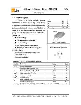
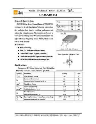
cs25n06 b4.pdf

Silicon N-Channel Power MOSFET R CS25N06 B4 General Description VDSS 60 V CS25N06 B4, the silicon N-channel Enhanced VDMOSFETs, ID 25 A PD(TC=25 ) 50 W is obtained by the self-aligned planar Technology which reduce RDS(ON)Typ 28 m the conduction loss, improve switching performance and enhance the avalanche energy. The transistor can be used in variou power s
dhs025n06 dhs025n06e.pdf
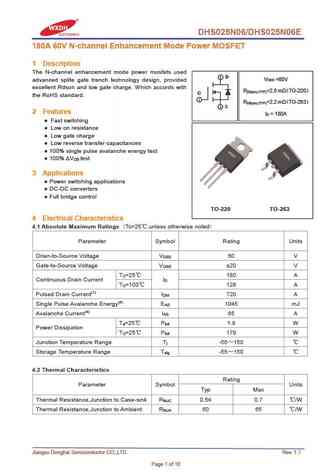
DHS025N06/DHS025N06E 180A 60V N-channel Enhancement Mode Power MOSFET 1 Description The N-channel enhancement mode power mosfets used 2 D V =60V DSS advanced splite gate trench technology design, provided excellent Rdson and low gate charge. Which accords with R =2.5 m TO-220 DS(on) (TYP) G the RoHS standard. 1 R =2.2 m TO-263 DS(on) (TYP) 3 S 2 Features I =
ndt25n06.pdf
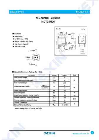
SMD Type MOSFET N-Channel MOSFET NDT25N06 TO-252 Unit mm +0.15 6.50-0.15 +0.1 2.30 -0.1 +0.2 Features 5.30-0.2 +0.8 0.50 -0.7 VDS (V) = 60V ID = 25 A (VGS = 10V) RDS(ON) 65m (VGS = 10V) 0.127 +0.1 0.80-0.1 max High Current Capability Low Gate Charge + 0.1 2.3 0.60- 0.1 1 Gate +0.15 2.Drain 4 .60 -0.15 2 Drain 3 Source 1.Gate 3.So
hyg025n06ls1p.pdf
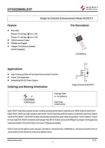
HYG025N06LS1P Single N-Channel Enhancement Mode MOSFET Feature Pin Description 60V/160A RDS(ON)= 2.5 m (typ.) @ VGS = 10V RDS(ON)= 3.7 m (typ.) @ VGS = 4.5V 100% Avalanche Tested Reliable and Rugged Halogen- Free Devices Available (RoHS Compliant) TO-220FB-3L Applications High Frequency Point-of-Load Synchronous Buck Converter Power Tool Application
hyg025n06ls1c2.pdf
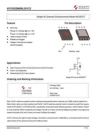
HYG025N06LS1C2 Single N-Channel Enhancement Mode MOSFET Feature Pin Description D D D D D D D D 60V/170A RDS(ON)= 2.1 m (typ.) @ VGS = 10V RDS(ON)= 3.2 m (typ.) @ VGS = 4.5V 100% Avalanche Tested Reliable and Rugged Halogen- Free Devices Available S S S G G S S S (RoHS Compliant) Pin1 PDFN8L 5x6 Applications High Frequency Point-of-Load Synchronous B
me25n06 me25n06-g.pdf
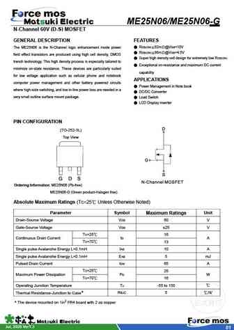
ME25N06/ME25N06-G N-Channel 60V (D-S) MOSFET GENERAL DESCRIPTION FEATURES RDS(ON) 62m @VGS=10V The ME25N06 is the N-Channel logic enhancement mode power RDS(ON) 86m @VGS=4.5V field effect transistors are produced using high cell density, DMOS Super high density cell design for extremely low RDS(ON) trench technology. This high density process is especially tailored
hrld125n06k hrlu125n06k.pdf
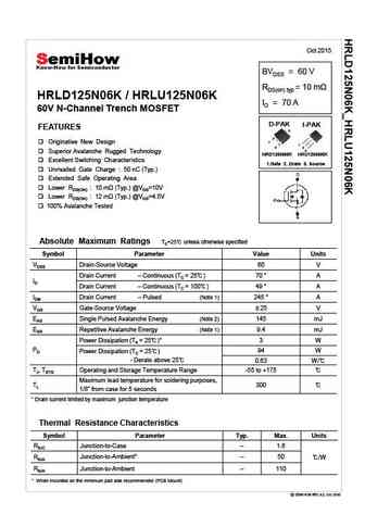
Oct 2015 BVDSS = 60 V RDS(on) typ = 10 HRLD125N06K / HRLU125N06K ID = 70 A 60V N-Channel Trench MOSFET D-PAK I-PAK FEATURES 2 1 Originative New Design 1 3 2 3 Superior Avalanche Rugged Technology HRD125N06K HRU125N06K Excellent Switching Characteristics 1.Gate 2. Drain 3. Source Unrivalled Gate Charge 50 nC (Typ.) Extended Safe Operating Area Lower RDS(ON)
hrlp125n06k.pdf
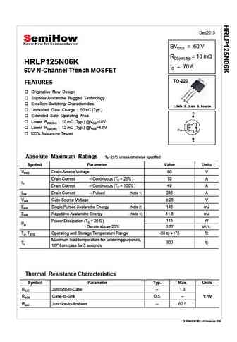
Dec2015 BVDSS = 60 V RDS(on) typ = 10 HRLP125N06K ID = 70 A 60V N-Channel Trench MOSFET TO-220 FEATURES Originative New Design Superior Avalanche Rugged Technology 1 2 3 Excellent Switching Characteristics 1.Gate 2. Drain 3. Source Unrivalled Gate Charge 50 nC (Typ.) Extended Safe Operating Area Lower RDS(ON) 10 (Typ.) @VGS=10V Lower RDS(ON) 12 (Typ.
hrlf125n06k.pdf
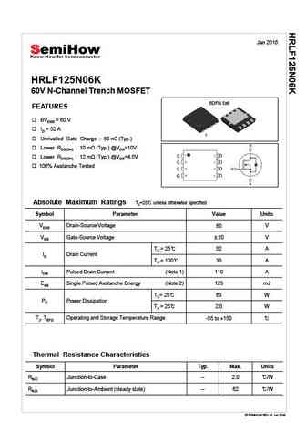
Jan 2016 HRLF125N06K 60V N-Channel Trench MOSFET 8DFN 5x6 FEATURES BVDSS = 60 V ID = 52 A 1 Unrivalled Gate Charge 50 nC (Typ.) Lower RDS(ON) 10 (Typ.) @VGS=10V Lower RDS(ON) 12 (Typ.) @VGS=4.5V 100% Avalanche Tested Absolute Maximum Ratings TJ=25 unless otherwise specified Symbol Parameter Value Units VDSS Drain-Source Voltage 60 V VGS Gate-Source Voltage 2
hrlo125n06k.pdf
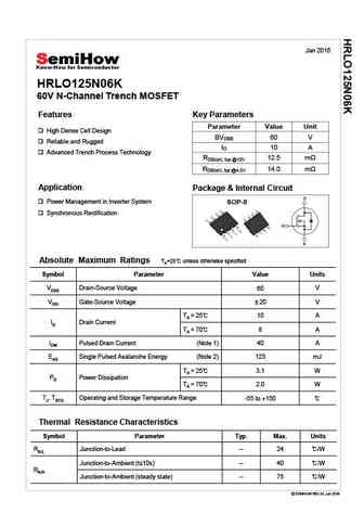
Jan 2016 HRLO125N06K 60V N-Channel Trench MOSFET Features Key Parameters Parameter Value Unit High Dense Cell Design BVDSS 60 V Reliable and Rugged ID 10 A Advanced Trench Process Technology RDS(on), typ @10V 12.5 RDS(on), typ @4.5V 14.0 Application Package & Internal Circuit Power Management in Inverter System SOP-8 Synchronous Rectification Absolute Maximum Ratings
25n06.pdf
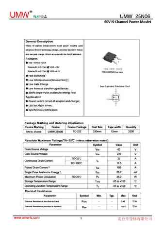
R UMW UMW 25N06 60V N-Channel Power Mosfet General Description These N-channel enhancement mode power mosfets used advanced trench technology design, provided excellent Rdson and low gate charge. Which accords with the RoHS standard. Features VDS = 60V,ID =25A RDS(ON),23 m (Typ) @ VGS =10V RDS(ON),30 m (Typ) @ VGS =4.5V Fast Switching Low ON Resistance(Rdson 29m ) Low Gate C
wmb025n06lg4.pdf
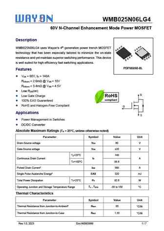
WMB025N06LG4 60V N-Channel Enhancement Mode Power MOSFET Description D D D D WMB025N06LG4 uses Wayon's 4th generation power trench MOSFET D D D D technology that has been especially tailored to minimize the on-state G ss resistance and yet maintain superior switching performance. This device s ss G s is well suited for high efficiency fast switching applications. PDFN5
wmk25n06ts.pdf
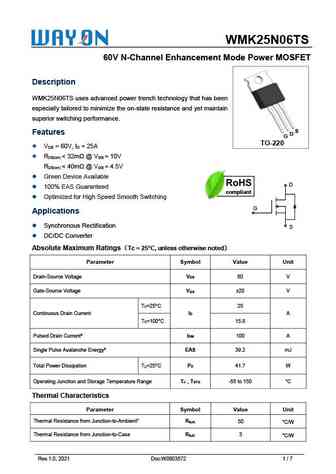
WMK25N06TS 60V N-Channel Enhancement Mode Power MOSFET Description WMK25N06TS uses advanced power trench technology that has been especially tailored to minimize the on-state resistance and yet maintain superior switching performance. S Features D G TO-220 V = 60V, I = 25A DS D R
wmo25n06ts.pdf
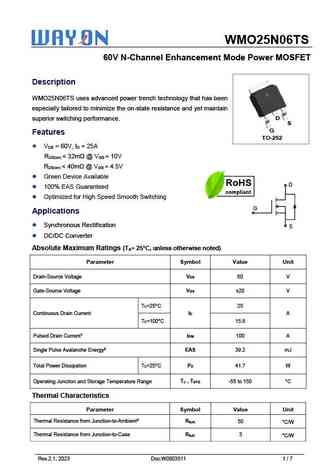
WMO25N06TS 60V N-Channel Enhancement Mode Power MOSFET Description WMO25N06TS uses advanced power trench technology that has been especially tailored to minimize the on-state resistance and yet maintain D superior switching performance. S G Features TO-252 V = 60V, I = 25A DS D R
wmb025n06hg4.pdf
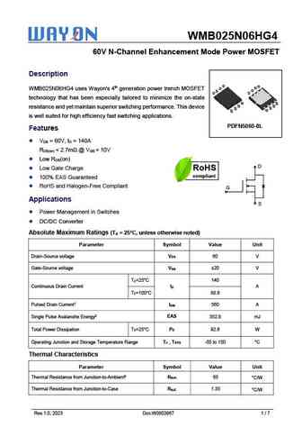
WMB025N06HG4 60V N-Channel Enhancement Mode Power MOSFET Description D D D D WMB025N06HG4 uses Wayon's 4th generation power trench MOSFET D D D D technology that has been especially tailored to minimize the on-state G ss resistance and yet maintain superior switching performance. This device s ss G s is well suited for high efficiency fast switching applications. PDFN5
cs25n06c4.pdf
Silicon N-Channel Power MOSFET R CS25N06 C4 General Description CS25N06 C4 the silicon N-channel Enhanced VDSS 60 V VDMOSFETs, is obtained by the high density Trench ID 25 A technology which reduce the conduction loss, improve switching PD 36.2 W RDS(ON)Typ 23 m performance and enhance the avalanche energy. This device is suitable for use as a load switch and P
cs25n06b4.pdf
Silicon N-Channel Power MOSFET R CS25N06 B4 General Description VDSS 60 V CS25N06 B4, the silicon N-channel Enhanced VDMOSFETs, ID 25 A PD(TC=25 ) 50 W is obtained by the self-aligned planar Technology which reduce RDS(ON)Typ 28 m the conduction loss, improve switching performance and enhance the avalanche energy. The transistor can be used in variou power s
hgb025n06s hgk025n06s hgp025n06s.pdf
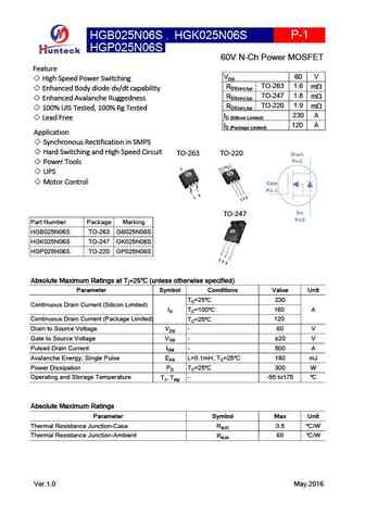
, HGB025N06S HGK025N06S P-1 HGP025N06S 60V N-Ch Power MOSFET Feature 60 V VDS High Speed Power Switching TO-263 1.6 RDS(on),typ m Enhanced Body diode dv/dt capability TO-247 1.8 RDS(on),typ m Enhanced Avalanche Ruggedness TO-220 1.9 RDS(on),typ m 100% UIS Tested, 100% Rg Tested 230 A ID (Sillicon Limited) Lead Free 120 A ID (Package Limited) Ap
hga025n06s.pdf
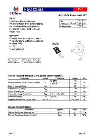
HGA025N06S P-1 60V N-Ch Power MOSFET Feature 60 V VDS High Speed Power Switching TO-220F 1.9 RDS(on),typ m Enhanced Body diode dv/dt capability 109 A ID (Sillicon Limited) Enhanced Avalanche Ruggedness 100% UIS Tested, 100% Rg Tested Lead Free Application Synchronous Rectification in SMPS Hard Switching and High Speed Circuit Drain Pin2 Powe
sud25n06-45l.pdf
SUD25N06-45L www.VBsemi.tw N-Channel 6 0-V (D-S) MOSFET FEATURES PRODUCT SUMMARY TrenchFET Power MOSFET VDS (V) rDS(on) ( ) ID (A)a Available 175 C Junction Temperature 0.025 at VGS = 10 V 35 RoHS* 60 0.030 at VGS = 4.5 V 30 COMPLIANT TO-252 D G Drain Connected to Tab G D S S Top View N-Channel MOSFET ABSOLUTE MAXIMUM RATINGS TC = 25 C, unless otherwis
25n06l-tn3.pdf
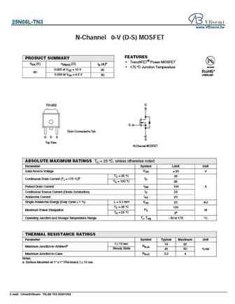
25N06L-TN3 www.VBsemi.tw N-Channel 6 0-V (D-S) MOSFET FEATURES PRODUCT SUMMARY TrenchFET Power MOSFET VDS (V) rDS(on) ( ) ID (A)a Available 175 C Junction Temperature 0.025 at VGS = 10 V 35 RoHS* 60 0.030 at VGS = 4.5 V 30 COMPLIANT TO-252 D G Drain Connected to Tab G D S S Top View N-Channel MOSFET ABSOLUTE MAXIMUM RATINGS TC = 25 C, unless otherwise no
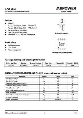
hm25n06q.pdf
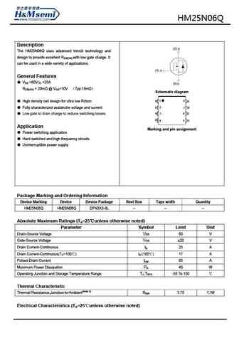
HM25N06Q Description The HM25N06Q uses advanced trench technology and design to provide excellent RDS(ON) with low gate charge. It can be used in a wide variety of applications. General Features VDS >60V,ID =25A RDS(ON)
hm25n06d.pdf
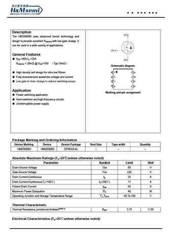
HM25N06D Description The HM25N06D uses advanced trench technology and design to provide excellent RDS(ON) with low gate charge. It can be used in a wide variety of applications. General Features VDS >60V,ID =25A RDS(ON)
ipd025n06n.pdf
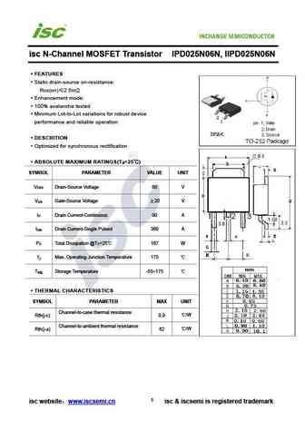
isc N-Channel MOSFET Transistor IPD025N06N, IIPD025N06N FEATURES Static drain-source on-resistance RDS(on) 2.5m Enhancement mode 100% avalanche tested Minimum Lot-to-Lot variations for robust device performance and reliable operation DESCRITION Optimized for synchronous rectification ABSOLUTE MAXIMUM RATINGS(T =25 ) a SYMBOL PARAMETER VALUE UNIT V Drain-Sou
fdi025n06.pdf
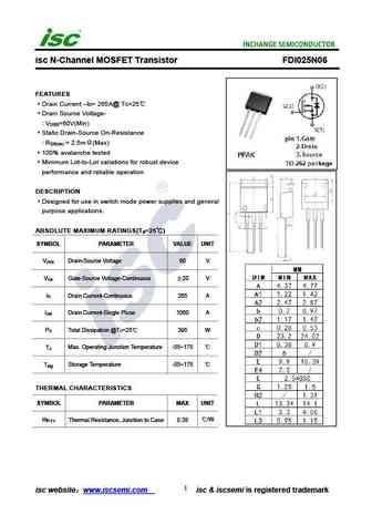
isc N-Channel MOSFET Transistor FDI025N06 FEATURES Drain Current I = 265A@ T =25 D C Drain Source Voltage- V =60V(Min) DSS Static Drain-Source On-Resistance R = 2.5m (Max) DS(on) 100% avalanche tested Minimum Lot-to-Lot variations for robust device performance and reliable operation DESCRIPTION Designed for use in switch mode power supplies and general purp
Otros transistores... 12N65B , 12N65H , 12N65TF , 13N50MF , 150N06Y , 16N65MF , 18N50MF , 20N65NF , AON7403 , 47N60YS , 4N60B , 4N60H , 4N65F , 4N65B , 4N65H , 4N65G , 4N65D .
🌐 : EN ES РУ

Liste
Recientemente añadidas las descripciónes de los transistores:
MOSFET: ASD80R750E | ASD70R950E | ASD70R600E | ASD70R380E | ASD65R850E | ASD65R550E | ASD65R350E | ASD65R300E | ASD65R280E | ASD65R270E | ASD60R330E | ASD60R280E | ASB80R750E | ASB70R380E | ASB65R300E | ASB65R220E
Popular searches
mp20a transistor | mrf450 | oc70 transistor | p0603bd mosfet | p157r5nt | ptp03n04n | sm4377 mosfet datasheet | tip31c reemplazo