ME2320D MOSFET Equivalente. Reemplazo. Hoja de especificaciones. Principales características
Número de Parte: ME2320D
Tipo de FET: MOSFET
Polaridad de transistor: N
ESPECIFICACIONES MÁXIMAS
Pdⓘ - Máxima disipación de potencia: 1.4 W
|Vds|ⓘ - Voltaje máximo drenador-fuente: 20 V
|Vgs|ⓘ - Voltaje máximo fuente-puerta: 8 V
|Id|ⓘ - Corriente continua de drenaje: 6.4 A
Tjⓘ - Temperatura máxima de unión: 150 °C
CARACTERÍSTICAS ELÉCTRICAS
trⓘ - Tiempo de subida: 420 nS
Cossⓘ - Capacitancia de salida: 95 pF
RDSonⓘ - Resistencia estado encendido drenaje a fuente: 0.021 Ohm
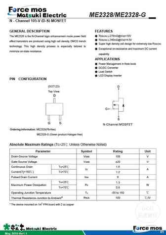
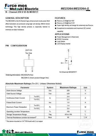
Encapsulados: SOT-23
Búsqueda de reemplazo de ME2320D MOSFET
- Selecciónⓘ de transistores por parámetros
ME2320D datasheet
me2320d me2320d-g.pdf
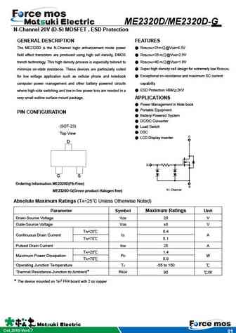
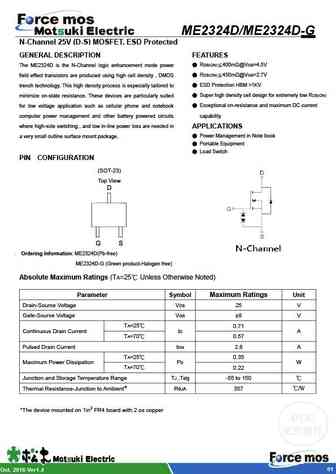
ME2320D/ME2320D-G N-Channel 20V (D-S) MOSFET , ESD Protection GENERAL DESCRIPTION FEATURES The ME2320D is the N-Channel logic enhancement mode power RDS(ON)=21m @VGS=4.5V field effect transistors are produced using high cell density, DMOS RDS(ON)=25 m @VGS=2.5V trench technology. This high density process is especially tailored to RDS(ON)=40 m @VGS=1.8V minimize on-st
me2320ds me2320ds-g.pdf
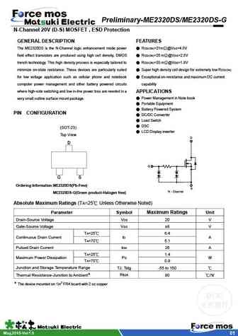
Preliminary-ME2320DS/ME2320DS-G N-Channel 20V (D-S) MOSFET , ESD Protection GENERAL DESCRIPTION FEATURES The ME2320DS is the N-Channel logic enhancement mode power RDS(ON)=21m @VGS=4.5V field effect transistors are produced using high cell density, DMOS RDS(ON)=25 m @VGS=2.5V trench technology. This high density process is especially tailored to RDS(ON)=33 m @VGS=1.8V
me2320d2-g me2320d2-g.pdf
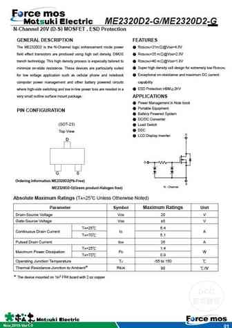
ME2320D2-G/ME2320D2-G N-Channel 20V (D-S) MOSFET , ESD Protection GENERAL DESCRIPTION FEATURES The ME2320D2 is the N-Channel logic enhancement mode power RDS(ON)=21m @VGS=4.5V field effect transistors are produced using high cell density, DMOS RDS(ON)=25 m @VGS=2.5V trench technology. This high density process is especially tailored to RDS(ON)=40 m @VGS=1.8V minimize on-s
me2323d me2323d-g.pdf
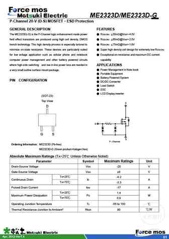
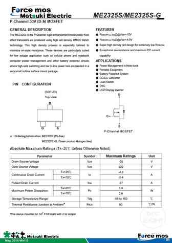
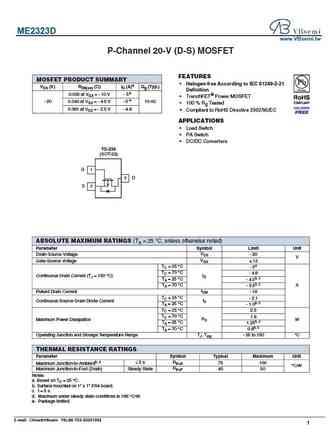
ME2323D/ME2323D-G P-Channel 20-V (D-S) MOSFET ESD Protection GENERAL DESCRIPTION FEATURES The ME2323D(-G) is the P-Channel logic enhancement mode power RDS(ON) 50m @VGS=-4.5V field effect transistors are produced using high cell density, DMOS RDS(ON) 65m @VGS=-2.5V trench technology. This high density process is especially tailored to RDS(ON) 75m @VGS=-1.8
Otros transistores... ME2306D , ME2306D-G , ME2307 , ME2307-G , ME2308S , ME2308S-G , ME2309 , ME2309-G , TK10A60D , ME2320D-G , ME2323D , ME2323D-G , ME2325 , ME2325-G , ME2326A , ME2326A-G , ME2328 .
History: AO4402G | IRF321 | 2N65L-TMA-T | BRCS70N08IP | SI2305CDS-T1-GE3 | STB17N80K5 | 2N6788L
History: AO4402G | IRF321 | 2N65L-TMA-T | BRCS70N08IP | SI2305CDS-T1-GE3 | STB17N80K5 | 2N6788L
🌐 : EN ES РУ

Liste
Recientemente añadidas las descripciónes de los transistores:
MOSFET: AUB034N10 | AUB033N08BG | AUB026N085 | AUA062N08BG | AUA060N08AG | AUA056N08BGL | AUA039N10 | ASW80R290E | ASW65R120EFD | ASW65R110E | ASW65R095EFD | ASW65R046EFD | ASW65R041EFDA | ASW65R041E | ASW60R150E | ASW60R090EFDA
Popular searches
a562 transistor | oc44 datasheet | 2sa70 | 2sa706 | 2sc539 | 2n5401 transistor equivalent | p0903bdg | c1384 transistor