NVMFS5A160PLZ MOSFET Equivalente. Reemplazo. Hoja de especificaciones. Principales características
Número de Parte: NVMFS5A160PLZ
Tipo de FET: MOSFET
Polaridad de transistor: P
ESPECIFICACIONES MÁXIMAS
Pdⓘ - Máxima disipación de potencia: 200 W
|Vds|ⓘ - Voltaje máximo drenador-fuente: 60 V
|Vgs|ⓘ - Voltaje máximo fuente-puerta: 20 V
|Id|ⓘ - Corriente continua de drenaje: 100 A
Tjⓘ - Temperatura máxima de unión: 175 °C
CARACTERÍSTICAS ELÉCTRICAS
trⓘ - Tiempo de subida: 690 nS
Cossⓘ - Capacitancia de salida: 720 pF
RDSonⓘ - Resistencia estado encendido drenaje a fuente: 0.0077 Ohm
Encapsulados: DFN5
Búsqueda de reemplazo de NVMFS5A160PLZ MOSFET
- Selecciónⓘ de transistores por parámetros
NVMFS5A160PLZ datasheet
nvmfs5a160plz.pdf
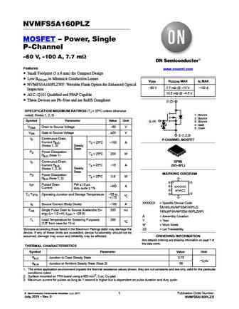
NVMFS5A160PLZ MOSFET Power, Single P-Channel -60 V, -100 A, 7.7 mW Features www.onsemi.com Small Footprint (5 x 6 mm) for Compact Design Low RDS(on) to Minimize Conduction Losses VDSS RDS(ON) MAX ID MAX NVMFS5A160PLZWF Wettable Flank Option for Enhanced Optical -60 V 7.7 mW @ -10 V -100 A Inspection 10.5 mW @ -4.5 V AEC-Q101 Qualified and PPAP Capable Thes
nvmfs5a140plz.pdf
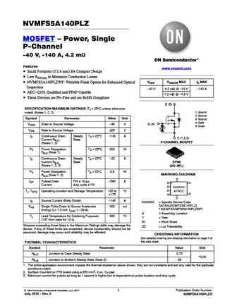
NVMFS5A140PLZ MOSFET Power, Single P-Channel -40 V, -140 A, 4.2 mW Features www.onsemi.com Small Footprint (5 x 6 mm) for Compact Design Low RDS(on) to Minimize Conduction Losses NVMFS5A140PLZWF Wettable Flank Option for Enhanced Optical VDSS RDS(ON) MAX ID MAX Inspection -40 V 4.2 mW @ -10 V -140 A AEC-Q101 Qualified and PPAP Capable 7.2 mW @ -4.5 V These
nvmfs5c450nl.pdf

NVMFS5C450NL Power MOSFET 40 V, 2.8 mW, 110 A, Single N-Channel Features Small Footprint (5x6 mm) for Compact Design Low RDS(on) to Minimize Conduction Losses www.onsemi.com Low QG and Capacitance to Minimize Driver Losses NVMFS5C450NLWF - Wettable Flank Option for Enhanced Optical Inspection V(BR)DSS RDS(ON) MAX ID MAX AEC-Q101 Qualified and PPAP Capable 2.8 mW
nvmfs5c404nl.pdf
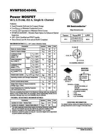
NVMFS5C404NL Power MOSFET 40 V, 0.75 mW, 352 A, Single N-Channel Features Small Footprint (5x6 mm) for Compact Design Low RDS(on) to Minimize Conduction Losses http //onsemi.com Low QG and Capacitance to Minimize Driver Losses NVMFS5C404NLWF - Wettable Flank Option for Enhanced Optical Inspection V(BR)DSS RDS(ON) MAX ID MAX AEC-Q101 Qualified and PPAP Capable 0.7
nvmfs5c460n.pdf
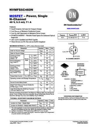
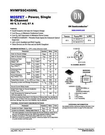
NVMFS5C460N MOSFET Power, Single N-Channel 40 V, 5.3 mW, 71 A Features www.onsemi.com Small Footprint (5x6 mm) for Compact Design Low RDS(on) to Minimize Conduction Losses Low QG and Capacitance to Minimize Driver Losses V(BR)DSS RDS(ON) MAX ID MAX NVMFS5C460NWF - Wettable Flank Option for Enhanced Optical Inspection 40 V 5.3 mW @ 10 V 71 A AEC-Q101 Qualified
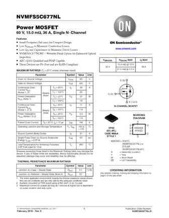
nvmfs5c670n.pdf
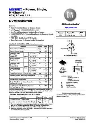
MOSFET Power, Single, N-Channel 60 V, 7.0 mW, 71 A NVMFS5C670N Features www.onsemi.com Small Footprint (5x6 mm) for Compact Design Low RDS(on) to Minimize Conduction Losses Low QG and Capacitance to Minimize Driver Losses V(BR)DSS RDS(ON) MAX ID MAX NVMFS5C670NWF - Wettable Flank Option for Enhanced Optical 60 V 7.0 mW @ 10 V 71 A Inspection AEC-Q101 Qualifi
nvmfs5832nl.pdf
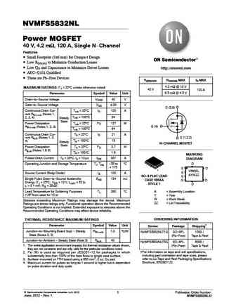
NVMFS5832NL Power MOSFET 40 V, 4.2 mW, 120 A, Single N-Channel Features Small Footprint (5x6 mm) for Compact Design Low RDS(on) to Minimize Conduction Losses Low QG and Capacitance to Minimize Driver Losses http //onsemi.com AEC-Q101 Qualified These are Pb-Free Devices V(BR)DSS RDS(ON) MAX ID MAX 4.2 mW @ 10 V MAXIMUM RATINGS (TJ = 25 C unless otherwise noted)
nvmfs5c604nl.pdf
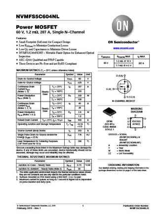
NVMFS5C604NL Power MOSFET 60 V, 1.2 mW, 287 A, Single N-Channel Features Small Footprint (5x6 mm) for Compact Design Low RDS(on) to Minimize Conduction Losses www.onsemi.com Low QG and Capacitance to Minimize Driver Losses NVMFS5C604NLWF - Wettable Flank Option for Enhanced Optical Inspection V(BR)DSS RDS(ON) MAX ID MAX AEC-Q101 Qualified and PPAP Capable 1.2 mW
nvmfs5h663nl nvmfs5h663nlwf.pdf

NVMFS5H663NL, NVMFS5H663NLWF MOSFET Power, Single N-Channel 60 V, 7.2 mW, 67 A www.onsemi.com NVMFS5H663NLWF - Wettable Flank Option for Enhanced Optical Inspection. V(BR)DSS RDS(ON) MAX ID MAX Features Small Footprint (5x6 mm) for Compact Design 7.2 mW @ 10 V 60 V 67 A Low RDS(on) to Minimize Conduction Losses 10 mW @ 4.5 V Low QG and Capacitance to Minimize Dri
nvmfs5c680nl.pdf
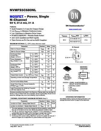
NVMFS5C680NL MOSFET Power, Single N-Channel 60 V, 27.5 mW, 21 A Features Small Footprint (5 x 6 mm) for Compact Design www.onsemi.com Low RDS(on) to Minimize Conduction Losses Low Capacitance to Minimize Driver Losses NVMFS5C680NLWF - Wettable Flanks Product V(BR)DSS RDS(on) MAX ID MAX AEC-Q101 Qualified and PPAP Capable 27.5 mW @ 10 V 60 V 21 A These D
ntmfs5834nl nvmfs5834nl.pdf
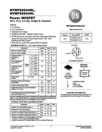
NTMFS5834NL, NVMFS5834NL Power MOSFET 40 V, 75 A, 9.3 mW, Single N-Channel Features Low RDS(on) Low Capacitance http //onsemi.com Optimized Gate Charge NVMFS5834NLWF - Wettable Flanks Product V(BR)DSS RDS(ON) MAX ID MAX NVMFS Prefix for Automotive and Other Applications Requiring 9.3 mW @ 10 V Unique Site and Control Change Requirements; AEC-Q101 40 V 75 A 13.6
nvmfs5c460nl.pdf

NVMFS5C460NL MOSFET Power, Single N-Channel 40 V, 4.5 mW, 78 A Features www.onsemi.com Small Footprint (5x6 mm) for Compact Design Low RDS(on) to Minimize Conduction Losses Low QG and Capacitance to Minimize Driver Losses V(BR)DSS RDS(ON) MAX ID MAX NVMFS5C460NLWF - Wettable Flank Option for Enhanced Optical 4.5 mW @ 10 V Inspection 40 V 78 A 7.2 mW @ 4.5 V
nvmfs5c410nl.pdf
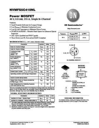
NVMFS5C410NL Power MOSFET 40 V, 0.9 mW, 315 A, Single N-Channel Features Small Footprint (5x6 mm) for Compact Design Low RDS(on) to Minimize Conduction Losses http //onsemi.com Low QG and Capacitance to Minimize Driver Losses NVMFS5C410NLWF - Wettable Flank Option for Enhanced Optical Inspection V(BR)DSS RDS(ON) MAX ID MAX AEC-Q101 Qualified and PPAP Capable 0.9
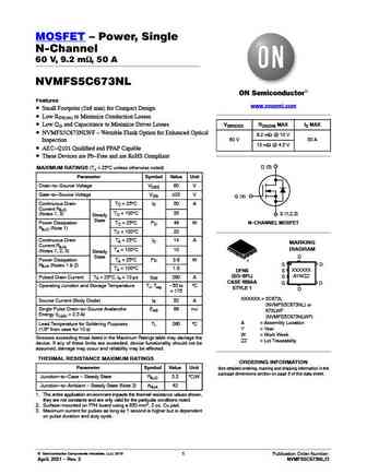
nvmfs5c673n.pdf
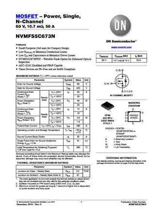
MOSFET Power, Single, N-Channel 60 V, 10.7 mW, 50 A NVMFS5C673N Features www.onsemi.com Small Footprint (5x6 mm) for Compact Design Low RDS(on) to Minimize Conduction Losses Low QG and Capacitance to Minimize Driver Losses V(BR)DSS RDS(ON) MAX ID MAX NVMFS5C673NWF - Wettable Flank Option for Enhanced Optical 60 V 10.7 mW @ 10 V 50 A Inspection AEC-Q101 Quali
nvmfs5c628n.pdf
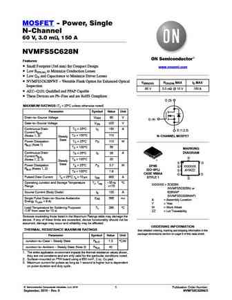
MOSFET - Power, Single N-Channel 60 V, 3.0 mW, 150 A NVMFS5C628N Features Small Footprint (5x6 mm) for Compact Design www.onsemi.com Low RDS(on) to Minimize Conduction Losses Low QG and Capacitance to Minimize Driver Losses NVMFS5C628NWF - Wettable Flank Option for Enhanced Optical V(BR)DSS RDS(ON) MAX ID MAX Inspection 60 V 3.0 mW @ 10 V 150 A AEC-Q101 Qualifie
nvmfs5c638nl.pdf
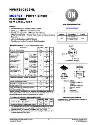
NVMFS5C638NL MOSFET Power, Single N-Channel 60 V, 3.0 mW, 133 A Features www.onsemi.com Small Footprint (5x6 mm) for Compact Design Low RDS(on) to Minimize Conduction Losses Low QG and Capacitance to Minimize Driver Losses V(BR)DSS RDS(ON) MAX ID MAX NVMFS5C638NLWF - Wettable Flank Option for Enhanced Optical 3.0 mW @ 10 V Inspection 60 V 133 A AEC-Q101 Qua
nvmfs5833n.pdf
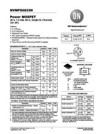
NVMFS5833N Power MOSFET 40 V, 7.5 mW, 86 A, Single N-Channel, SO-8FL Features Low RDS(on) http //onsemi.com Low Capacitance Optimized Gate Charge V(BR)DSS RDS(ON) MAX ID MAX AEC-Q101 Qualified and PPAP Capable NVMFS5833NWF - Wettable Franks Option for Enhanced Optical 40 V 7.5 mW @ 10 V 86 A Inspection These Devices are Pb-Free and are RoHS Compliant D (5)
nvmfs5h600nl.pdf
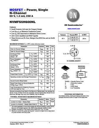
MOSFET Power, Single N-Channel 60 V, 1.3 mW, 250 A NVMFS5H600NL Features www.onsemi.com Small Footprint (5x6 mm) for Compact Design Low RDS(on) to Minimize Conduction Losses Low QG and Capacitance to Minimize Driver Losses V(BR)DSS RDS(ON) MAX ID MAX AEC-Q101 Qualified and PPAP Capable 1.3 mW @ 10 V These Devices are Pb-Free, Halogen Free/BFR Free and are RoH
nvmfs5c468n.pdf
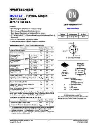
NVMFS5C468N MOSFET Power, Single N-Channel 40 V, 12 mW, 35 A Features www.onsemi.com Small Footprint (5x6 mm) for Compact Design Low RDS(on) to Minimize Conduction Losses Low QG and Capacitance to Minimize Driver Losses V(BR)DSS RDS(ON) MAX ID MAX NVMFS5C468NWF - Wettable Flank Option for Enhanced Optical 40 V 12 mW @ 10 V 35 A Inspection AEC-Q101 Qualified
nvmfs5c404n.pdf
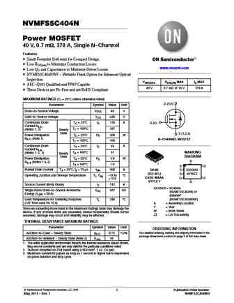
NVMFS5C404N Power MOSFET 40 V, 0.7 mW, 378 A, Single N-Channel Features Small Footprint (5x6 mm) for Compact Design Low RDS(on) to Minimize Conduction Losses www.onsemi.com Low QG and Capacitance to Minimize Driver Losses NVMFS5C404NWF - Wettable Flank Option for Enhanced Optical Inspection V(BR)DSS RDS(ON) MAX ID MAX AEC-Q101 Qualified and PPAP Capable 40 V 0.7
nvmfs5c682nl.pdf

NVMFS5C682NL MOSFET Power, Single N-Channel 60 V, 21 mW, 25 A Features www.onsemi.com Small Footprint (5x6 mm) for Compact Design Low RDS(on) to Minimize Conduction Losses Low QG and Capacitance to Minimize Driver Losses V(BR)DSS RDS(ON) MAX ID MAX NVMFS5C682NLWF - Wettable Flank Option for Enhanced Optical 21 mW @ 10 V 60 V 25 A Inspection 31.5 mW @ 4.5 V
nvmfs5c673nl.pdf
MOSFET Power, Single N-Channel 60 V, 9.2 mW, 50 A NVMFS5C673NL Features www.onsemi.com Small Footprint (5x6 mm) for Compact Design Low RDS(on) to Minimize Conduction Losses Low QG and Capacitance to Minimize Driver Losses V(BR)DSS RDS(ON) MAX ID MAX NVMFS5C673NLWF - Wettable Flank Option for Enhanced Optical 9.2 mW @ 10 V 60 V 50 A Inspection 13 mW @ 4.5 V
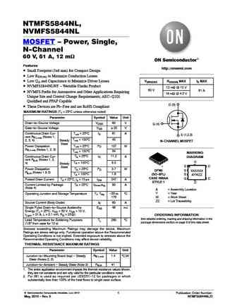
nvmfs5830nl.pdf
NVMFS5830NL Power MOSFET 40 V, 2.3 mW, 185 A, Single N-Channel Features Small Footprint (5x6 mm) for Compact Design Low RDS(on) to Minimize Conduction Losses http //onsemi.com Low QG and Capacitance to Minimize Driver Losses NVMFS5830NLWF - Wettable Flanks Product V(BR)DSS RDS(ON) MAX ID MAX AEC-Q101 Qualified and PPAP Capable These Devices are Pb-Free and are
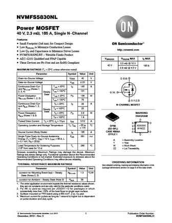
ntmfs5844nl nvmfs5844nl.pdf
NTMFS5844NL, NVMFS5844NL MOSFET Power, Single, N-Channel 60 V, 61 A, 12 mW Features http //onsemi.com Small Footprint (5x6 mm) for Compact Design Low RDS(on) to Minimize Conduction Losses Low QG and Capacitance to Minimize Driver Losses V(BR)DSS RDS(ON) MAX ID MAX NVMFS5844NLWF - Wettable Flanks Product 12 mW @ 10 V 60 V 61 A NVMFS Prefix for Automotive and
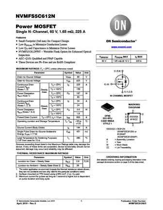
nvmfs5c612nl.pdf

NVMFS5C612NL Power MOSFET 60 V, 1.5 mW, 235 A, Single N-Channel Features Small Footprint (5x6 mm) for Compact Design Low RDS(on) to Minimize Conduction Losses www.onsemi.com Low QG and Capacitance to Minimize Driver Losses NVMFS5C612NLWF - Wettable Flank Option for Enhanced Optical Inspection V(BR)DSS RDS(ON) MAX ID MAX AEC-Q101 Qualified and PPAP Capable 1.5 mW
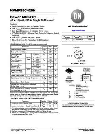
nvmfs5c426nl.pdf
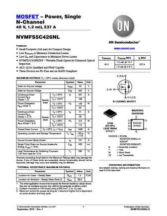
MOSFET Power, Single N-Channel 40 V, 1.2 mW, 237 A NVMFS5C426NL Features www.onsemi.com Small Footprint (5x6 mm) for Compact Design Low RDS(on) to Minimize Conduction Losses Low QG and Capacitance to Minimize Driver Losses V(BR)DSS RDS(ON) MAX ID MAX NVMFS5C426NLWF - Wettable Flank Option for Enhanced Optical 1.2 mW @ 10 V Inspection 40 V 237 A 1.8 mW @ 4.5 V
nvmfs5885nl.pdf
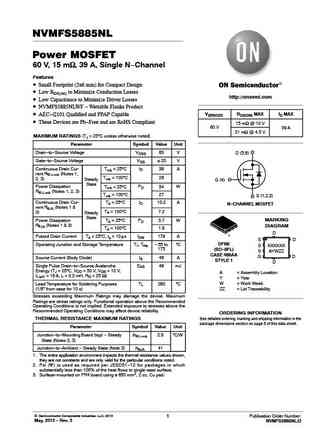
NVMFS5885NL Power MOSFET 60 V, 15 mW, 39 A, Single N-Channel Features Small Footprint (5x6 mm) for Compact Design Low RDS(on) to Minimize Conduction Losses http //onsemi.com Low Capacitance to Minimize Driver Losses NVMFS5885NLWF - Wettable Flanks Product V(BR)DSS RDS(ON) MAX ID MAX AEC-Q101 Qualified and PPAP Capable These Devices are Pb-Free and are RoHS Com
nvmfs5c612n.pdf
NVMFS5C612N Power MOSFET Single N-Channel, 60 V, 1.65 mW, 225 A Features Small Footprint (5x6 mm) for Compact Design Low RDS(on) to Minimize Conduction Losses www.onsemi.com Low QG and Capacitance to Minimize Driver Losses NVMFS5C612NWF - Wettable Flank Option for Enhanced Optical Inspection V(BR)DSS RDS(ON) MAX ID MAX AEC-Q101 Qualified and PPAP Capable 60 V 1.6
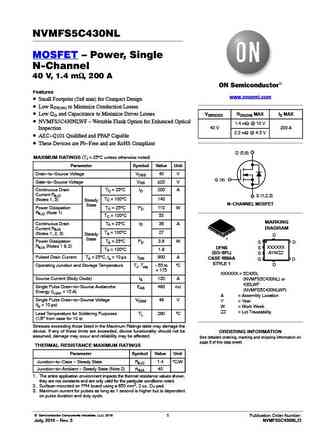
nvmfs5c430n.pdf
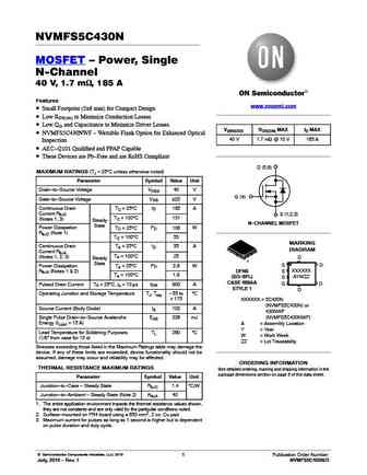
NVMFS5C430N MOSFET Power, Single N-Channel 40 V, 1.7 mW, 185 A Features www.onsemi.com Small Footprint (5x6 mm) for Compact Design Low RDS(on) to Minimize Conduction Losses Low QG and Capacitance to Minimize Driver Losses V(BR)DSS RDS(ON) MAX ID MAX NVMFS5C430NWF - Wettable Flank Option for Enhanced Optical 40 V 1.7 mW @ 10 V 185 A Inspection AEC-Q101 Qualif
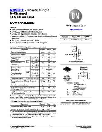
nvmfs5c406nl.pdf
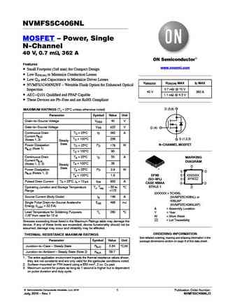
NVMFS5C406NL MOSFET Power, Single N-Channel 40 V, 0.7 mW, 362 A Features www.onsemi.com Small Footprint (5x6 mm) for Compact Design Low RDS(on) to Minimize Conduction Losses Low QG and Capacitance to Minimize Driver Losses V(BR)DSS RDS(ON) MAX ID MAX NVMFS5C406NLWF - Wettable Flank Option for Enhanced Optical 0.7 mW @ 10 V Inspection 40 V 362 A AEC-Q101 Qua
nvmfs5c423nl.pdf
NVMFS5C423NL Power MOSFET 40 V, 2.0 mW, 150 A, Single N-Channel Features Small Footprint (5x6 mm) for Compact Design Low RDS(on) to Minimize Conduction Losses www.onsemi.com Low QG and Capacitance to Minimize Driver Losses NVMFS5C423NLWF - Wettable Flank Option for Enhanced Optical Inspection V(BR)DSS RDS(ON) MAX ID MAX AEC-Q101 Qualified and PPAP Capable 2.0 mW
nvmfs5c468nl.pdf

NVMFS5C468NL MOSFET Power, Single N-Channel 40 V, 10.3 mW, 37 A Features www.onsemi.com Small Footprint (5x6 mm) for Compact Design Low RDS(on) to Minimize Conduction Losses Low QG and Capacitance to Minimize Driver Losses V(BR)DSS RDS(ON) MAX ID MAX NVMFS5C468NLWF - Wettable Flank Option for Enhanced Optical 10.3 mW @ 10 V Inspection 40 V 37 A 17.6 mW @ 4.5 V
nvmfs5c466n.pdf

NVMFS5C466N MOSFET Power, Single N-Channel 40 V, 8.1 mW, 49 A Features www.onsemi.com Small Footprint (5x6 mm) for Compact Design Low RDS(on) to Minimize Conduction Losses Low QG and Capacitance to Minimize Driver Losses V(BR)DSS RDS(ON) MAX ID MAX NVMFS5C466NWF - Wettable Flank Option for Enhanced Optical 40 V 8.1 mW @ 10 V 49 A Inspection AEC-Q101 Qualifie
nvmfs5h663nl.pdf
NVMFS5H663NL, NVMFS5H663NLWF MOSFET Power, Single N-Channel 60 V, 7.2 mW, 67 A www.onsemi.com NVMFS5H663NLWF - Wettable Flank Option for Enhanced Optical Inspection. V(BR)DSS RDS(ON) MAX ID MAX Features Small Footprint (5x6 mm) for Compact Design 7.2 mW @ 10 V 60 V 67 A Low RDS(on) to Minimize Conduction Losses 10 mW @ 4.5 V Low QG and Capacitance to Minimize Dri
nvmfs5c442n.pdf
NVMFS5C442N Power MOSFET 40 V, 2.3 mW, 140 A, Single N-Channel Features Small Footprint (5x6 mm) for Compact Design Low RDS(on) to Minimize Conduction Losses www.onsemi.com Low QG and Capacitance to Minimize Driver Losses NVMFS5C442NWF - Wettable Flank Option for Enhanced Optical Inspection V(BR)DSS RDS(ON) MAX ID MAX AEC-Q101 Qualified and PPAP Capable 40 V 2.3
nvmfs5c670nl.pdf
NVMFS5C670NL Power MOSFET 60 V, 6.1 mW, 71 A, Single N-Channel Features Small Footprint (5x6 mm) for Compact Design Low RDS(on) to Minimize Conduction Losses www.onsemi.com Low QG and Capacitance to Minimize Driver Losses NVMFS5C670NLWF - Wettable Flank Option for Enhanced Optical Inspection V(BR)DSS RDS(ON) MAX ID MAX AEC-Q101 Qualified and PPAP Capable 6.1 mW @
nvmfs5c645nl.pdf
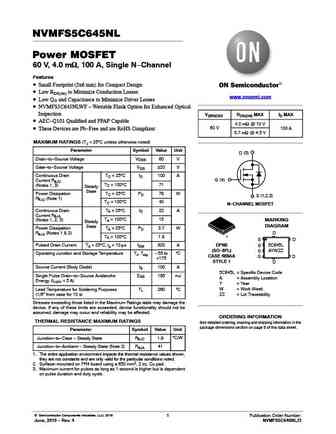
NVMFS5C645NL Power MOSFET 60 V, 4.0 mW, 100 A, Single N-Channel Features Small Footprint (5x6 mm) for Compact Design Low RDS(on) to Minimize Conduction Losses www.onsemi.com Low QG and Capacitance to Minimize Driver Losses NVMFS5C645NLWF - Wettable Flank Option for Enhanced Optical Inspection V(BR)DSS RDS(ON) MAX ID MAX AEC-Q101 Qualified and PPAP Capable 4.0 mW
nvmfs5c442nl.pdf
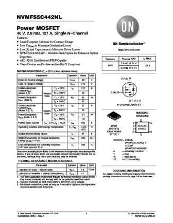
NVMFS5C442NL Power MOSFET 40 V, 2.8 mW, 127 A, Single N-Channel Features Small Footprint (5x6 mm) for Compact Design Low RDS(on) to Minimize Conduction Losses Low QG and Capacitance to Minimize Driver Losses http //onsemi.com NVMFS5C442NLWF - Wettable Flank Option for Enhanced Optical Inspection V(BR)DSS RDS(ON) MAX ID MAX AEC-Q101 Qualified and PPAP Capable 2.8
nvmfs5c406n.pdf
MOSFET - Power, Single N-Channel 40 V, 0.8 mW, 353 A NVMFS5C406N Features www.onsemi.com Small Footprint (5x6 mm) for Compact Design Low RDS(on) to Minimize Conduction Losses Low QG and Capacitance to Minimize Driver Losses NVMFS5C406NWF - Wettable Flank Option for Enhanced Optical V(BR)DSS RDS(ON) MAX ID MAX Inspection 40 V 0.8 mW @ 10 V 353 A AEC-Q101 Qualifie
nvmfs5c426n.pdf
NVMFS5C426N Power MOSFET 40 V, 1.3 mW, 235 A, Single N-Channel Features Small Footprint (5x6 mm) for Compact Design Low RDS(on) to Minimize Conduction Losses www.onsemi.com Low QG and Capacitance to Minimize Driver Losses NVMFS5C426NWF - Wettable Flank Option for Enhanced Optical Inspection V(BR)DSS RDS(ON) MAX ID MAX AEC-Q101 Qualified and PPAP Capable 40 V 1.3
nvmfs5c646nl.pdf
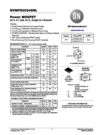
NVMFS5C646NL Power MOSFET 60 V, 4.7 mW, 93 A, Single N-Channel Features Small Footprint (5x6 mm) for Compact Design Low RDS(on) to Minimize Conduction Losses www.onsemi.com Low QG and Capacitance to Minimize Driver Losses NVMFS5C646NLWF - Wettable Flank Option for Enhanced Optical Inspection V(BR)DSS RDS(ON) MAX ID MAX AEC-Q101 Qualified and PPAP Capable 4.7 mW @
nvmfs5834nl.pdf
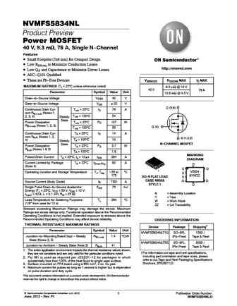
NVMFS5834NL Product Preview Power MOSFET 40 V, 9.3 mW, 76 A, Single N-Channel Features Small Footprint (5x6 mm) for Compact Design Low RDS(on) to Minimize Conduction Losses http //onsemi.com Low QG and Capacitance to Minimize Driver Losses AEC-Q101 Qualified These are Pb-Free Devices V(BR)DSS RDS(ON) MAX ID MAX MAXIMUM RATINGS (TJ = 25 C unless otherwise noted)
nvmfs5c450n.pdf
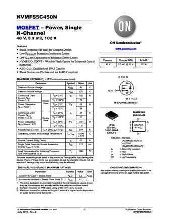
NVMFS5C450N MOSFET Power, Single N-Channel 40 V, 3.3 mW, 102 A Features www.onsemi.com Small Footprint (5x6 mm) for Compact Design Low RDS(on) to Minimize Conduction Losses Low QG and Capacitance to Minimize Driver Losses V(BR)DSS RDS(ON) MAX ID MAX NVMFS5C450NWF - Wettable Flank Option for Enhanced Optical 40 V 3.3 mW @ 10 V 102 A Inspection AEC-Q101 Qualif
nvmfs5113pl.pdf
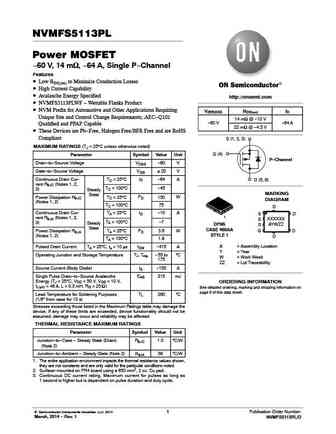
NVMFS5113PL Power MOSFET -60 V, 14 mW, -64 A, Single P-Channel Features Low RDS(on) to Minimize Conduction Losses High Current Capability Avalanche Energy Specified http //onsemi.com NVMFS5113PLWF - Wettable Flanks Product NVM Prefix for Automotive and Other Applications Requiring V(BR)DSS RDS(on) ID Unique Site and Control Change Requirements; AEC-Q101 14 mW @ -
nvmfs5826nl.pdf
NVMFS5826NL Power MOSFET 60 V, 24 mW, 26 A, Single N-Channel Features Small Footprint (5x6 mm) for Compact Design Low RDS(on) to Minimize Conduction Losses http //onsemi.com Low QG and Capacitance to Minimize Driver Losses AEC-Q101 Qualified and PPAP Capable These are Pb-Free Devices and RoHS Compliant V(BR)DSS RDS(ON) MAX ID MAX 24 mW @ 10 V 60 V MAXIMUM RATINGS
ntmfs5844nlt1g nvmfs5844nl.pdf
NTMFS5844NL, NVMFS5844NL Power MOSFET 60 V, 61 A, 12 mW, Single N-Channel Features Small Footprint (5x6 mm) for Compact Design http //onsemi.com Low RDS(on) to Minimize Conduction Losses Low QG and Capacitance to Minimize Driver Losses NVMFS Prefix for Automotive and Other Applications Requiring V(BR)DSS RDS(ON) MAX ID MAX Unique Site and Control Change Requirements;
nvmfs5c456n.pdf
MOSFET Power, Single N-Channel 40 V, 4.5 mW, 80 A NVMFS5C456N Features www.onsemi.com Small Footprint (5x6 mm) for Compact Design Low RDS(on) to Minimize Conduction Losses Low QG and Capacitance to Minimize Driver Losses V(BR)DSS RDS(ON) MAX ID MAX NVMFS5C456NWF - Wettable Flank Option for Enhanced Optical 40 V 4.5 mW @ 10 V 80 A Inspection AEC-Q101 Qualifie
nvmfs5c410n.pdf

MOSFET - Power, Single N-Channel 40 V, 0.92 mW, 300 A NVMFS5C410N Features www.onsemi.com Small Footprint (5x6 mm) for Compact Design Low RDS(on) to Minimize Conduction Losses Low QG and Capacitance to Minimize Driver Losses NVMFS5C410NWF - Wettable Flank Option for Enhanced Optical V(BR)DSS RDS(ON) MAX ID MAX Inspection 40 V 0.92 mW @ 10 V 300 A AEC-Q101 Qualif
Otros transistores... NVMFS015N10MCL, NVMFS016N06C, NVMFS020N06C, NVMFS024N06C, NVMFS3D6N10MCL, NVMFS4C302N, NVMFS4C310N, NVMFS5A140PLZ, 8205A, NVMFS5C406N, NVMFS5C406NL, NVMFS5C410N, NVMFS5C426N, NVMFS5C426NL, NVMFS5C430N, NVMFS5C430NL, NVMFS5C442N
History: AOT8N80
🌐 : EN ES РУ

Liste
Recientemente añadidas las descripciónes de los transistores:
MOSFET: FTF30P35D | FTF25N35DHVT | FTF15N35D | FTE15C35G | FTP02P15G | FTE02P15G | AKF30N5P0SX | AKF30N10S | AKF20P45D | CM4407 | CM3407 | CM3400 | SVF11N65F | SVF11N65T | FKBB3105 | EHBA036R1
Popular searches
bdw93c equivalent | cs7n60f | d613 transistor | fdmc8884 mosfet | k3569 mosfet equivalent | 2sa1370 | 4508nh mosfet | a94 transistor