NVMFS5C426NL MOSFET Equivalente. Reemplazo. Hoja de especificaciones. Principales características
Número de Parte: NVMFS5C426NL
Tipo de FET: MOSFET
Polaridad de transistor: N
ESPECIFICACIONES MÁXIMAS
Pdⓘ - Máxima
disipación de potencia: 128 W
|Vds|ⓘ - Voltaje máximo drenador-fuente: 40 V
|Vgs|ⓘ - Voltaje máximo fuente-puerta: 20 V
|Id|ⓘ - Corriente continua
de drenaje: 237 A
Tjⓘ - Temperatura máxima de unión: 175 °C
CARACTERÍSTICAS ELÉCTRICAS
trⓘ - Tiempo
de subida: 72 nS
Cossⓘ - Capacitancia de salida: 2600 pF
RDSonⓘ - Resistencia estado encendido drenaje a fuente: 0.0012 Ohm
Encapsulados: DFN5
Búsqueda de reemplazo de NVMFS5C426NL MOSFET
- Selecciónⓘ de transistores por parámetros
NVMFS5C426NL datasheet
..1. Size:177K onsemi
nvmfs5c426nl.pdf 
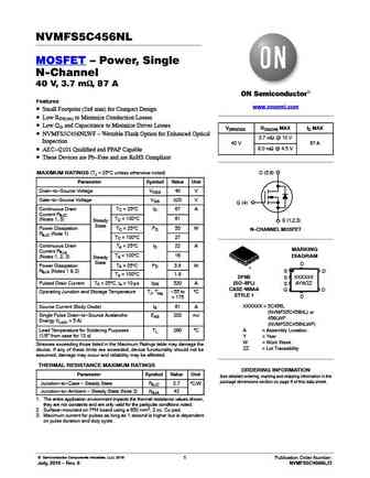
MOSFET Power, Single N-Channel 40 V, 1.2 mW, 237 A NVMFS5C426NL Features www.onsemi.com Small Footprint (5x6 mm) for Compact Design Low RDS(on) to Minimize Conduction Losses Low QG and Capacitance to Minimize Driver Losses V(BR)DSS RDS(ON) MAX ID MAX NVMFS5C426NLWF - Wettable Flank Option for Enhanced Optical 1.2 mW @ 10 V Inspection 40 V 237 A 1.8 mW @ 4.5 V
3.1. Size:118K onsemi
nvmfs5c426n.pdf
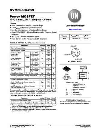
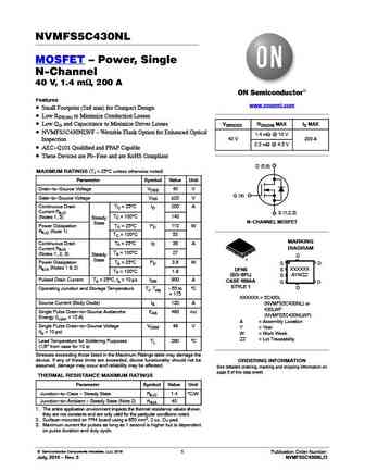
NVMFS5C426N Power MOSFET 40 V, 1.3 mW, 235 A, Single N-Channel Features Small Footprint (5x6 mm) for Compact Design Low RDS(on) to Minimize Conduction Losses www.onsemi.com Low QG and Capacitance to Minimize Driver Losses NVMFS5C426NWF - Wettable Flank Option for Enhanced Optical Inspection V(BR)DSS RDS(ON) MAX ID MAX AEC-Q101 Qualified and PPAP Capable 40 V 1.3
5.1. Size:123K onsemi
nvmfs5c423nl.pdf
NVMFS5C423NL Power MOSFET 40 V, 2.0 mW, 150 A, Single N-Channel Features Small Footprint (5x6 mm) for Compact Design Low RDS(on) to Minimize Conduction Losses www.onsemi.com Low QG and Capacitance to Minimize Driver Losses NVMFS5C423NLWF - Wettable Flank Option for Enhanced Optical Inspection V(BR)DSS RDS(ON) MAX ID MAX AEC-Q101 Qualified and PPAP Capable 2.0 mW
6.1. Size:160K onsemi
nvmfs5c450nl.pdf
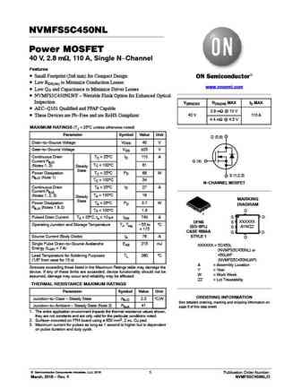
NVMFS5C450NL Power MOSFET 40 V, 2.8 mW, 110 A, Single N-Channel Features Small Footprint (5x6 mm) for Compact Design Low RDS(on) to Minimize Conduction Losses www.onsemi.com Low QG and Capacitance to Minimize Driver Losses NVMFS5C450NLWF - Wettable Flank Option for Enhanced Optical Inspection V(BR)DSS RDS(ON) MAX ID MAX AEC-Q101 Qualified and PPAP Capable 2.8 mW
6.2. Size:75K onsemi
nvmfs5c404nl.pdf
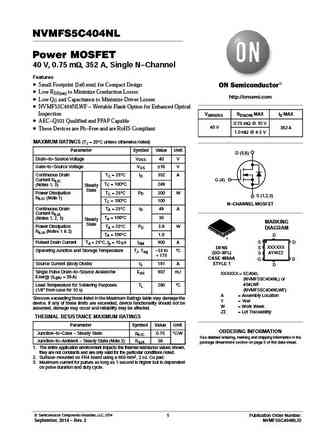
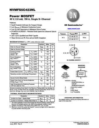
NVMFS5C404NL Power MOSFET 40 V, 0.75 mW, 352 A, Single N-Channel Features Small Footprint (5x6 mm) for Compact Design Low RDS(on) to Minimize Conduction Losses http //onsemi.com Low QG and Capacitance to Minimize Driver Losses NVMFS5C404NLWF - Wettable Flank Option for Enhanced Optical Inspection V(BR)DSS RDS(ON) MAX ID MAX AEC-Q101 Qualified and PPAP Capable 0.7
6.3. Size:180K onsemi
nvmfs5c460n.pdf
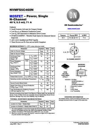
NVMFS5C460N MOSFET Power, Single N-Channel 40 V, 5.3 mW, 71 A Features www.onsemi.com Small Footprint (5x6 mm) for Compact Design Low RDS(on) to Minimize Conduction Losses Low QG and Capacitance to Minimize Driver Losses V(BR)DSS RDS(ON) MAX ID MAX NVMFS5C460NWF - Wettable Flank Option for Enhanced Optical Inspection 40 V 5.3 mW @ 10 V 71 A AEC-Q101 Qualified
6.5. Size:134K onsemi
nvmfs5c460nl.pdf

NVMFS5C460NL MOSFET Power, Single N-Channel 40 V, 4.5 mW, 78 A Features www.onsemi.com Small Footprint (5x6 mm) for Compact Design Low RDS(on) to Minimize Conduction Losses Low QG and Capacitance to Minimize Driver Losses V(BR)DSS RDS(ON) MAX ID MAX NVMFS5C460NLWF - Wettable Flank Option for Enhanced Optical 4.5 mW @ 10 V Inspection 40 V 78 A 7.2 mW @ 4.5 V
6.6. Size:71K onsemi
nvmfs5c410nl.pdf
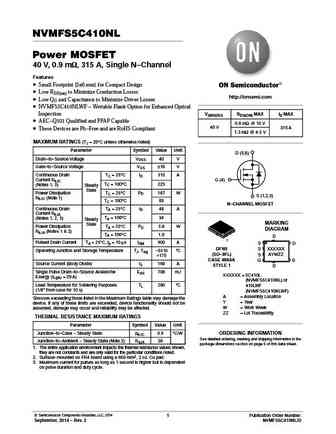
NVMFS5C410NL Power MOSFET 40 V, 0.9 mW, 315 A, Single N-Channel Features Small Footprint (5x6 mm) for Compact Design Low RDS(on) to Minimize Conduction Losses http //onsemi.com Low QG and Capacitance to Minimize Driver Losses NVMFS5C410NLWF - Wettable Flank Option for Enhanced Optical Inspection V(BR)DSS RDS(ON) MAX ID MAX AEC-Q101 Qualified and PPAP Capable 0.9
6.7. Size:174K onsemi
nvmfs5c468n.pdf
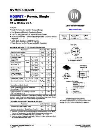
NVMFS5C468N MOSFET Power, Single N-Channel 40 V, 12 mW, 35 A Features www.onsemi.com Small Footprint (5x6 mm) for Compact Design Low RDS(on) to Minimize Conduction Losses Low QG and Capacitance to Minimize Driver Losses V(BR)DSS RDS(ON) MAX ID MAX NVMFS5C468NWF - Wettable Flank Option for Enhanced Optical 40 V 12 mW @ 10 V 35 A Inspection AEC-Q101 Qualified
6.8. Size:70K onsemi
nvmfs5c404n.pdf
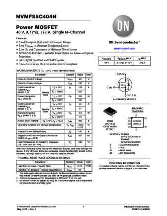
NVMFS5C404N Power MOSFET 40 V, 0.7 mW, 378 A, Single N-Channel Features Small Footprint (5x6 mm) for Compact Design Low RDS(on) to Minimize Conduction Losses www.onsemi.com Low QG and Capacitance to Minimize Driver Losses NVMFS5C404NWF - Wettable Flank Option for Enhanced Optical Inspection V(BR)DSS RDS(ON) MAX ID MAX AEC-Q101 Qualified and PPAP Capable 40 V 0.7
6.9. Size:173K onsemi
nvmfs5c430n.pdf
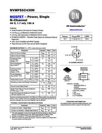
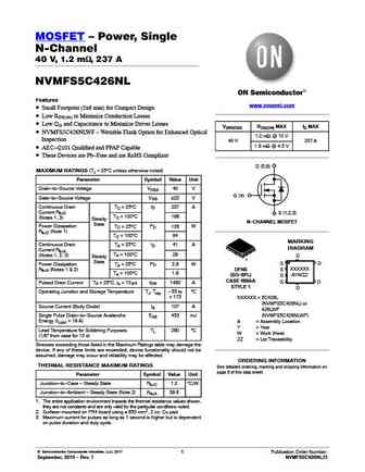
NVMFS5C430N MOSFET Power, Single N-Channel 40 V, 1.7 mW, 185 A Features www.onsemi.com Small Footprint (5x6 mm) for Compact Design Low RDS(on) to Minimize Conduction Losses Low QG and Capacitance to Minimize Driver Losses V(BR)DSS RDS(ON) MAX ID MAX NVMFS5C430NWF - Wettable Flank Option for Enhanced Optical 40 V 1.7 mW @ 10 V 185 A Inspection AEC-Q101 Qualif
6.10. Size:191K onsemi
nvmfs5c406nl.pdf
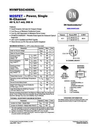
NVMFS5C406NL MOSFET Power, Single N-Channel 40 V, 0.7 mW, 362 A Features www.onsemi.com Small Footprint (5x6 mm) for Compact Design Low RDS(on) to Minimize Conduction Losses Low QG and Capacitance to Minimize Driver Losses V(BR)DSS RDS(ON) MAX ID MAX NVMFS5C406NLWF - Wettable Flank Option for Enhanced Optical 0.7 mW @ 10 V Inspection 40 V 362 A AEC-Q101 Qua
6.12. Size:173K onsemi
nvmfs5c468nl.pdf
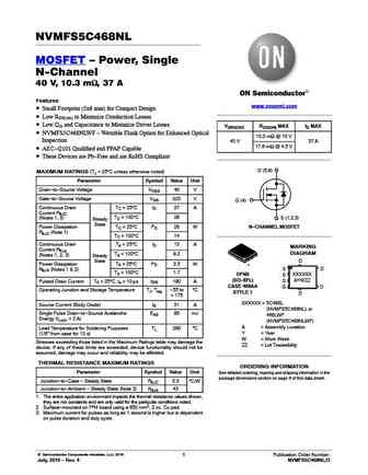
NVMFS5C468NL MOSFET Power, Single N-Channel 40 V, 10.3 mW, 37 A Features www.onsemi.com Small Footprint (5x6 mm) for Compact Design Low RDS(on) to Minimize Conduction Losses Low QG and Capacitance to Minimize Driver Losses V(BR)DSS RDS(ON) MAX ID MAX NVMFS5C468NLWF - Wettable Flank Option for Enhanced Optical 10.3 mW @ 10 V Inspection 40 V 37 A 17.6 mW @ 4.5 V
6.13. Size:134K onsemi
nvmfs5c466n.pdf

NVMFS5C466N MOSFET Power, Single N-Channel 40 V, 8.1 mW, 49 A Features www.onsemi.com Small Footprint (5x6 mm) for Compact Design Low RDS(on) to Minimize Conduction Losses Low QG and Capacitance to Minimize Driver Losses V(BR)DSS RDS(ON) MAX ID MAX NVMFS5C466NWF - Wettable Flank Option for Enhanced Optical 40 V 8.1 mW @ 10 V 49 A Inspection AEC-Q101 Qualifie
6.14. Size:181K onsemi
nvmfs5c442n.pdf
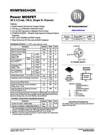
NVMFS5C442N Power MOSFET 40 V, 2.3 mW, 140 A, Single N-Channel Features Small Footprint (5x6 mm) for Compact Design Low RDS(on) to Minimize Conduction Losses www.onsemi.com Low QG and Capacitance to Minimize Driver Losses NVMFS5C442NWF - Wettable Flank Option for Enhanced Optical Inspection V(BR)DSS RDS(ON) MAX ID MAX AEC-Q101 Qualified and PPAP Capable 40 V 2.3
6.15. Size:73K onsemi
nvmfs5c442nl.pdf
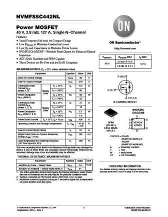
NVMFS5C442NL Power MOSFET 40 V, 2.8 mW, 127 A, Single N-Channel Features Small Footprint (5x6 mm) for Compact Design Low RDS(on) to Minimize Conduction Losses Low QG and Capacitance to Minimize Driver Losses http //onsemi.com NVMFS5C442NLWF - Wettable Flank Option for Enhanced Optical Inspection V(BR)DSS RDS(ON) MAX ID MAX AEC-Q101 Qualified and PPAP Capable 2.8
6.16. Size:177K onsemi
nvmfs5c406n.pdf
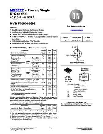
MOSFET - Power, Single N-Channel 40 V, 0.8 mW, 353 A NVMFS5C406N Features www.onsemi.com Small Footprint (5x6 mm) for Compact Design Low RDS(on) to Minimize Conduction Losses Low QG and Capacitance to Minimize Driver Losses NVMFS5C406NWF - Wettable Flank Option for Enhanced Optical V(BR)DSS RDS(ON) MAX ID MAX Inspection 40 V 0.8 mW @ 10 V 353 A AEC-Q101 Qualifie
6.17. Size:166K onsemi
nvmfs5c450n.pdf
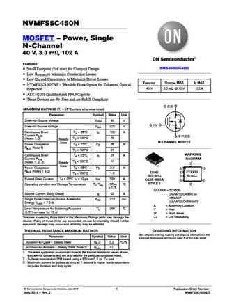
NVMFS5C450N MOSFET Power, Single N-Channel 40 V, 3.3 mW, 102 A Features www.onsemi.com Small Footprint (5x6 mm) for Compact Design Low RDS(on) to Minimize Conduction Losses Low QG and Capacitance to Minimize Driver Losses V(BR)DSS RDS(ON) MAX ID MAX NVMFS5C450NWF - Wettable Flank Option for Enhanced Optical 40 V 3.3 mW @ 10 V 102 A Inspection AEC-Q101 Qualif
6.18. Size:179K onsemi
nvmfs5c456n.pdf
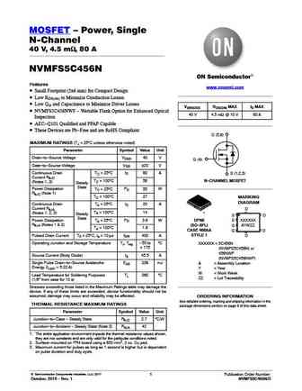
MOSFET Power, Single N-Channel 40 V, 4.5 mW, 80 A NVMFS5C456N Features www.onsemi.com Small Footprint (5x6 mm) for Compact Design Low RDS(on) to Minimize Conduction Losses Low QG and Capacitance to Minimize Driver Losses V(BR)DSS RDS(ON) MAX ID MAX NVMFS5C456NWF - Wettable Flank Option for Enhanced Optical 40 V 4.5 mW @ 10 V 80 A Inspection AEC-Q101 Qualifie
6.19. Size:171K onsemi
nvmfs5c410n.pdf
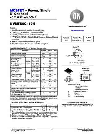
MOSFET - Power, Single N-Channel 40 V, 0.92 mW, 300 A NVMFS5C410N Features www.onsemi.com Small Footprint (5x6 mm) for Compact Design Low RDS(on) to Minimize Conduction Losses Low QG and Capacitance to Minimize Driver Losses NVMFS5C410NWF - Wettable Flank Option for Enhanced Optical V(BR)DSS RDS(ON) MAX ID MAX Inspection 40 V 0.92 mW @ 10 V 300 A AEC-Q101 Qualif
Otros transistores... NVMFS4C302N, NVMFS4C310N, NVMFS5A140PLZ, NVMFS5A160PLZ, NVMFS5C406N, NVMFS5C406NL, NVMFS5C410N, NVMFS5C426N, AON7408, NVMFS5C430N, NVMFS5C430NL, NVMFS5C442N, NVMFS5C450N, NVMFS5C450NL, NVMFS5C456N, NVMFS5C456NL, NVMFS5C460N