NVMFS6D1N08H Datasheet. Equivalente. Reemplazo. Hoja de especificaciones. Principales características
Número de Parte: NVMFS6D1N08H 📄📄
Tipo de FET: MOSFET
Polaridad de transistor: N
ESPECIFICACIONES MÁXIMAS
Pdⓘ - Máxima disipación de potencia: 104 W
|Vds|ⓘ - Voltaje máximo drenador-fuente: 80 V
|Vgs|ⓘ - Voltaje máximo fuente-puerta: 20 V
|Id|ⓘ - Corriente continua de drenaje: 89 A
Tjⓘ - Temperatura máxima de unión: 175 °C
CARACTERÍSTICAS ELÉCTRICAS
trⓘ - Tiempo de subida: 50 nS
Cossⓘ - Capacitancia de salida: 300 pF
RDSonⓘ - Resistencia estado encendido drenaje a fuente: 0.0055 Ohm
Encapsulados: DFN5
📄📄 Copiar
Búsqueda de reemplazo de NVMFS6D1N08H MOSFET
- Selecciónⓘ de transistores por parámetros
NVMFS6D1N08H datasheet
..1. Size:134K onsemi
nvmfs6d1n08h.pdf 
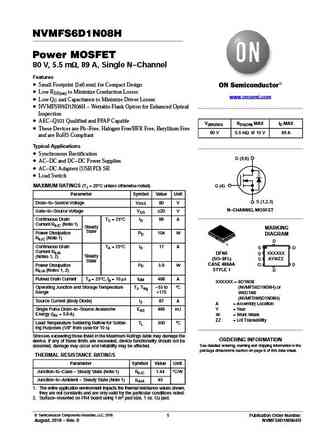
NVMFS6D1N08H Power MOSFET 80 V, 5.5 mW, 89 A, Single N-Channel Features Small Footprint (5x6 mm) for Compact Design Low RDS(on) to Minimize Conduction Losses www.onsemi.com Low QG and Capacitance to Minimize Driver Losses NVMFSW6D1N08H - Wettable Flank Option for Enhanced Optical Inspection AEC-Q101 Qualified and PPAP Capable V(BR)DSS RDS(ON) MAX ID MAX These
8.1. Size:174K onsemi
nvmfs6h858nl.pdf
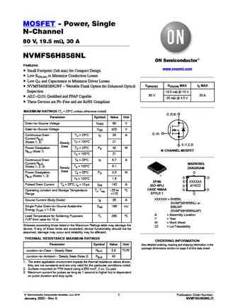
MOSFET - Power, Single N-Channel 80 V, 19.5 mW, 30 A NVMFS6H858NL Features www.onsemi.com Small Footprint (5x6 mm) for Compact Design Low RDS(on) to Minimize Conduction Losses Low QG and Capacitance to Minimize Driver Losses V(BR)DSS RDS(ON) MAX ID MAX NVMFS6H858NLWF - Wettable Flank Option for Enhanced Optical Inspection 19.5 mW @ 10 V 80 V 30 A AEC-Q101 Quali
8.2. Size:176K onsemi
nvmfs6h824n.pdf

MOSFET - Power, Single N-Channel 80 V, 4.5 mW, 107 A NVMFS6H824N Features www.onsemi.com Small Footprint (5x6 mm) for Compact Design Low RDS(on) to Minimize Conduction Losses Low QG and Capacitance to Minimize Driver Losses NVMFS6H824NWF - Wettable Flank Option for Enhanced Optical V(BR)DSS RDS(ON) MAX ID MAX Inspection 80 V 4.5 mW @ 10 V 107 A AEC-Q101 Qualifie
8.3. Size:174K onsemi
nvmfs6h818n.pdf
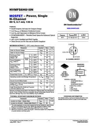
NVMFS6H818N MOSFET Power, Single N-Channel 80 V, 3.7 mW, 123 A Features www.onsemi.com Small Footprint (5x6 mm) for Compact Design Low RDS(on) to Minimize Conduction Losses Low QG and Capacitance to Minimize Driver Losses V(BR)DSS RDS(ON) MAX ID MAX NVMFS6H818NWF - Wettable Flank Option for Enhanced Optical Inspection 80 V 3.7 mW @ 10 V 123 A AEC-Q101 Qualif
8.4. Size:177K onsemi
nvmfs6h848n.pdf

MOSFET - Power, Single N-Channel 80 V, 9.4 mW, 64 A NVMFS6H848N Features www.onsemi.com Small Footprint (5x6 mm) for Compact Design Low RDS(on) to Minimize Conduction Losses Low QG and Capacitance to Minimize Driver Losses NVMFS6H848NWF - Wettable Flank Option for Enhanced Optical V(BR)DSS RDS(ON) MAX ID MAX Inspection 80 V 9.4 mW @ 10 V 64 A AEC-Q101 Qualified
8.5. Size:79K onsemi
nvmfs6b14nl.pdf
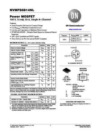
NVMFS6B14NL Power MOSFET 100 V, 13 mW, 55 A, Single N-Channel Features Small Footprint (5x6 mm) for Compact Design Low RDS(on) to Minimize Conduction Losses www.onsemi.com Low QG and Capacitance to Minimize Driver Losses NVMFS6B14NLWF - Wettable Flank Option for Enhanced Optical Inspection V(BR)DSS RDS(ON) MAX ID MAX AEC-Q101 Qualified and PPAP Capable 13 mW @ 10
8.6. Size:172K onsemi
nvmfs6h801nl.pdf

MOSFET - Power, Single N-Channel 80 V, 2.7 mW, 160 A NVMFS6H801NL Features www.onsemi.com Small Footprint (5x6 mm) for Compact Design Low RDS(on) to Minimize Conduction Losses Low QG and Capacitance to Minimize Driver Losses NVMFS6H801NLWF - Wettable Flank Option for Enhanced Optical V(BR)DSS RDS(ON) MAX ID MAX Inspection 2.7 mW @ 10 V AEC-Q101 Qualified and PPA
8.7. Size:178K onsemi
nvmfs6h852n.pdf
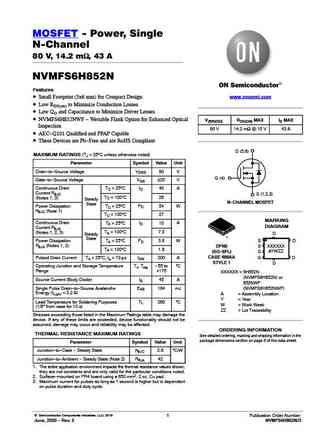
MOSFET - Power, Single N-Channel 80 V, 14.2 mW, 43 A NVMFS6H852N Features www.onsemi.com Small Footprint (5x6 mm) for Compact Design Low RDS(on) to Minimize Conduction Losses Low QG and Capacitance to Minimize Driver Losses NVMFS6H852NWF - Wettable Flank Option for Enhanced Optical V(BR)DSS RDS(ON) MAX ID MAX Inspection 80 V 14.2 mW @ 10 V 43 A AEC-Q101 Qualifie
8.8. Size:180K onsemi
nvmfs6h864n.pdf
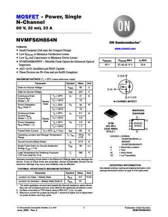
MOSFET - Power, Single N-Channel 80 V, 32 mW, 23 A NVMFS6H864N Features www.onsemi.com Small Footprint (5x6 mm) for Compact Design Low RDS(on) to Minimize Conduction Losses Low QG and Capacitance to Minimize Driver Losses V(BR)DSS RDS(ON) MAX ID MAX NVMFS6H864NWF - Wettable Flank Option for Enhanced Optical 80 V 32 mW @ 10 V 23 A Inspection AEC-Q101 Qualified an
8.9. Size:172K onsemi
nvmfs6h818nl.pdf
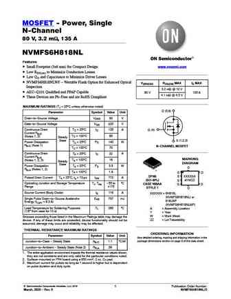
MOSFET - Power, Single N-Channel 80 V, 3.2 mW, 135 A NVMFS6H818NL Features www.onsemi.com Small Footprint (5x6 mm) for Compact Design Low RDS(on) to Minimize Conduction Losses Low QG and Capacitance to Minimize Driver Losses NVMFS6H818NLWF - Wettable Flank Option for Enhanced Optical V(BR)DSS RDS(ON) MAX ID MAX Inspection 3.2 mW @ 10 V AEC-Q101 Qualified and PPA
8.10. Size:203K onsemi
nvmfs6h801n.pdf

MOSFET Power, Single, N-Channel 80 V, 2.8 mW, 157 A NVMFS6H801N Features www.onsemi.com Small Footprint (5x6 mm) for Compact Design Low RDS(on) to Minimize Conduction Losses Low QG and Capacitance to Minimize Driver Losses V(BR)DSS RDS(ON) MAX ID MAX NVMFS6H801NWF - Wettable Flank Option for Enhanced Optical Inspection 80 V 2.8 mW @ 10 V 157 A AEC-Q101 Quali
8.11. Size:121K onsemi
nvmfs6b75nl.pdf
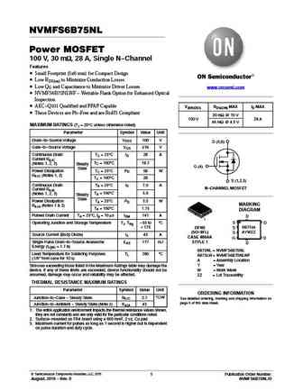
NVMFS6B75NL Power MOSFET 100 V, 30 mW, 28 A, Single N-Channel Features Small Footprint (5x6 mm) for Compact Design Low RDS(on) to Minimize Conduction Losses Low QG and Capacitance to Minimize Driver Losses www.onsemi.com NVMFS6B75NLWF - Wettable Flank Option for Enhanced Optical Inspection AEC-Q101 Qualified and PPAP Capable V(BR)DSS RDS(ON) MAX ID MAX These
8.12. Size:196K onsemi
nvmfs6h800nl.pdf
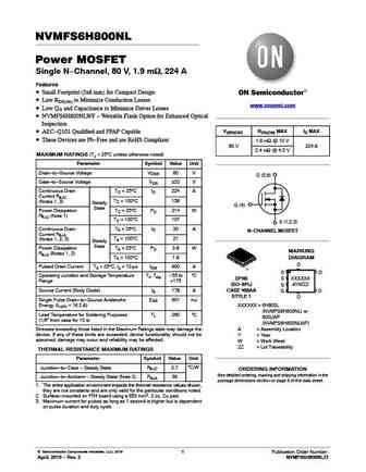
NVMFS6H800NL Power MOSFET Single N-Channel, 80 V, 1.9 mW, 224 A Features Small Footprint (5x6 mm) for Compact Design Low RDS(on) to Minimize Conduction Losses www.onsemi.com Low QG and Capacitance to Minimize Driver Losses NVMFS6H800NLWF - Wettable Flank Option for Enhanced Optical Inspection V(BR)DSS RDS(ON) MAX ID MAX AEC-Q101 Qualified and PPAP Capable The
8.13. Size:175K onsemi
nvmfs6h836nl.pdf

MOSFET - Power, Single N-Channel 80 V, 6.2 mW, 77 A NVMFS6H836NL Features www.onsemi.com Small Footprint (5x6 mm) for Compact Design Low RDS(on) to Minimize Conduction Losses Low QG and Capacitance to Minimize Driver Losses V(BR)DSS RDS(ON) MAX ID MAX NVMFS6H836NLWF - Wettable Flank Option for Enhanced Optical Inspection 6.2 mW @ 10 V 80 V 77 A AEC-Q101 Qualif
8.14. Size:176K onsemi
nvmfs6h836n.pdf

MOSFET - Power, Single N-Channel 80 V, 6.7 mW, 80 A NVMFS6H836N Features www.onsemi.com Small Footprint (5x6 mm) for Compact Design Low RDS(on) to Minimize Conduction Losses Low QG and Capacitance to Minimize Driver Losses V(BR)DSS RDS(ON) MAX ID MAX NVMFS6H836NWF - Wettable Flank Option for Enhanced Optical Inspection 80 V 6.7 mW @ 10 V 80 A AEC-Q101 Qualified
8.15. Size:175K onsemi
nvmfs6h824nl.pdf

MOSFET - Power, Single N-Channel 80 V, 4 mW, 110 A NVMFS6H824NL Features www.onsemi.com Small Footprint (5x6 mm) for Compact Design Low RDS(on) to Minimize Conduction Losses Low QG and Capacitance to Minimize Driver Losses V(BR)DSS RDS(ON) MAX ID MAX NVMFS6H824NLWF - Wettable Flank Option for Enhanced Optical Inspection 4 mW @ 10 V 80 V 110 A AEC-Q101 Qualified
8.16. Size:173K onsemi
nvmfs6h864nl.pdf

MOSFET - Power, Single N-Channel 80 V, 29 mW, 22 A NVMFS6H864NL Features www.onsemi.com Small Footprint (5x6 mm) for Compact Design Low RDS(on) to Minimize Conduction Losses Low QG and Capacitance to Minimize Driver Losses NVMFS6H864NLWF - Wettable Flank Option for Enhanced Optical V(BR)DSS RDS(ON) MAX ID MAX Inspection 29 mW @ 10 V AEC-Q101 Qualified and PPAP C
8.17. Size:176K onsemi
nvmfs6h848nl.pdf
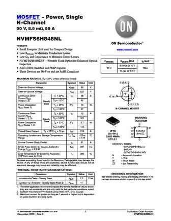
MOSFET - Power, Single N-Channel 80 V, 8.8 mW, 59 A NVMFS6H848NL Features www.onsemi.com Small Footprint (5x6 mm) for Compact Design Low RDS(on) to Minimize Conduction Losses Low QG and Capacitance to Minimize Driver Losses NVMFS6H848NLWF - Wettable Flank Option for Enhanced Optical V(BR)DSS RDS(ON) MAX ID MAX Inspection 8.8 mW @ 10 V AEC-Q101 Qualified and PPAP
8.18. Size:178K onsemi
nvmfs6h852nl.pdf
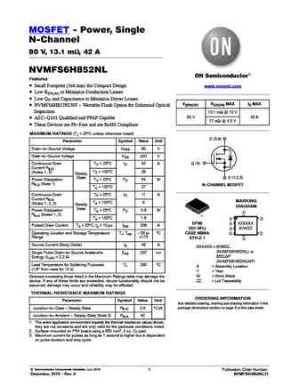
MOSFET - Power, Single N-Channel 80 V, 13.1 mW, 42 A NVMFS6H852NL Features Small Footprint (5x6 mm) for Compact Design www.onsemi.com Low RDS(on) to Minimize Conduction Losses Low QG and Capacitance to Minimize Driver Losses V(BR)DSS RDS(ON) MAX ID MAX NVMFS6H852NLWF - Wettable Flank Option for Enhanced Optical Inspection 13.1 mW @ 10 V 80 V 42 A AEC-Q101 Quali
8.19. Size:178K onsemi
nvmfs6h858n.pdf

MOSFET - Power, Single N-Channel 80 V, 20.7 mW, 32 A NVMFS6H858N Features www.onsemi.com Small Footprint (5x6 mm) for Compact Design Low RDS(on) to Minimize Conduction Losses Low QG and Capacitance to Minimize Driver Losses NVMFS6H858NWF - Wettable Flank Option for Enhanced Optical V(BR)DSS RDS(ON) MAX ID MAX Inspection 80 V 20.7 mW @ 10 V 32 A AEC-Q101 Qualifie
Otros transistores... NVMFS5C677NL, NVMFS5C680NL, NVMFS5C682NL, NVMFS5H600NL, NVMFS5H663NL, NVMFS5H663NLWF, NVMFS6B14NL, NVMFS6B75NL, CS150N04A8, NVMFS6H800NL, NVMFS6H801N, NVMFS6H801NL, NVMFS6H818N, NVMFS6H818NL, NVMFS6H824N, NVMFS6H824NL, NVMFS6H836N
