F10N65 MOSFET Equivalente. Reemplazo. Hoja de especificaciones. Principales características
Número de Parte: F10N65
Tipo de FET: MOSFET
Polaridad de transistor: N
ESPECIFICACIONES MÁXIMAS
Pdⓘ - Máxima
disipación de potencia: 38 W
|Vds|ⓘ - Voltaje máximo drenador-fuente: 650 V
|Vgs|ⓘ - Voltaje máximo fuente-puerta: 30 V
|Id|ⓘ - Corriente continua
de drenaje: 10 A
Tjⓘ - Temperatura máxima de unión: 150 °C
CARACTERÍSTICAS ELÉCTRICAS
trⓘ - Tiempo
de subida: 21 nS
Cossⓘ - Capacitancia de salida: 130 pF
RDSonⓘ - Resistencia estado encendido drenaje a fuente: 1 Ohm
Encapsulados: TO220F
Búsqueda de reemplazo de F10N65 MOSFET
- Selecciónⓘ de transistores por parámetros
F10N65 datasheet
..1. Size:1368K cn wxdh
f10n65.pdf 

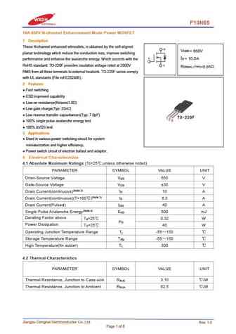
F10N65 10A 650V N-channel Enhancement Mode Power MOSFET 1 Description These N-channel enhanced vdmosfets, is obtained by the self-aligned V DSS = 650V planar technology which reduce the conduction loss, improve switching I = 10.0A D performance and enhance the avalanche energy. Which accords with the RoHS standard. TO-220F provides insulation voltage rated at 2000V R DS(on) TYP)
..2. Size:403K cn shandong jingdao microelectronics
f10n65.pdf 

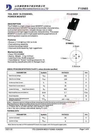
Jingdao Microelectronics co.LTD F10N65 ITO-220ABW 10A, 650V N-CHANNEL POWER MOSFET DESCRIPTION The F10N65 is a high voltage power MOSFET combines advanced trench MOSFET designed to have better characteristics, such as fast switching time, low gate charge, low on-state resistance and high rugged avalanche characteristics. This pow
0.1. Size:601K 1
svf10n65f svf10n65t.pdf 

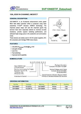
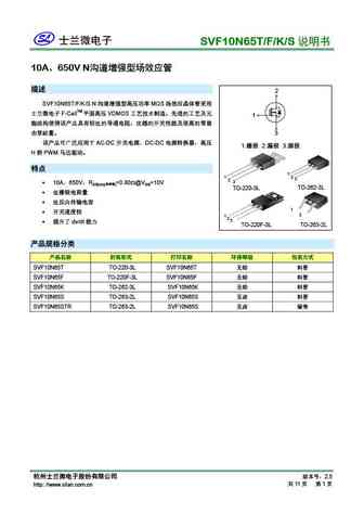
SVF10N65T/F_Datasheet 10A, 650V N-CHANNEL MOSFET GENERAL DESCRIPTION SVF10N65T/F is an N-channel enhancement mode power MOS field effect transistor which is produced using Silan proprietary F-CellTM structure VDMOS technology. The improved planar stripe cell and the improved guard ring terminal have been especially tailored to minimize on-state resistance, provide superior switch
0.3. Size:390K jiangsu
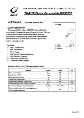
cjpf10n65.pdf 

JIANGSU CHANGJIANG ELECTRONICS TECHNOLOGY CO., LTD TO-220F Plastic-Encapsulate MOSFETS CJPF10N65 N-Channel Power MOSFET TO-220F GENERAL DESCRIPTION This advanced high voltage MOSFET is designed to stand high energy in the avalanche mode and switch efficiently. This new high energy device also offers a drain-to-source diode fast recovery time. Designed for high voltage, high s
0.4. Size:381K kec
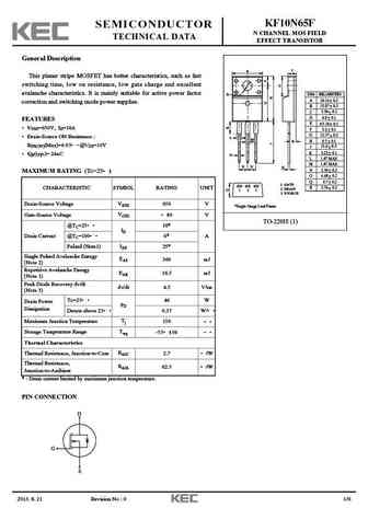
kf10n65f.pdf 

KF10N65F SEMICONDUCTOR N CHANNEL MOS FIELD TECHNICAL DATA EFFECT TRANSISTOR General Description C A This planar stripe MOSFET has better characteristics, such as fast switching time, low on resistance, low gate charge and excellent avalanche characteristics. It is mainly suitable for active power factor E DIM MILLIMETERS _ A 10.16 0.2 + correction and switching mode power suppli
0.5. Size:385K cet
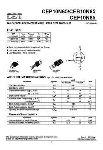
cep10n65 ceb10n65 cef10n65.pdf 

CEP10N65/CEB10N65 CEF10N65 N-Channel Enhancement Mode Field Effect Transistor PRELIMINARY FEATURES Type VDSS RDS(ON) ID @VGS CEP10N65 650V 0.85 10A 10V CEB10N65 650V 0.85 10A 10V CEF10N65 650V 0.85 10A d 10V D Super high dense cell design for extremely low RDS(ON). High power and current handing capability. Lead-free plating ; RoHS compliant. G S CEB SERIES CEP SERIES CE
0.6. Size:341K aosemi
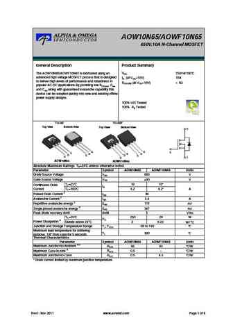
aowf10n65.pdf 

AOW10N65/AOWF10N65 650V,10A N-Channel MOSFET General Description Product Summary VDS 750V@150 The AOW10N65/AOWF10N65 is fabricated using an advanced high voltage MOSFET process that is designed ID (at VGS=10V) 10A to deliver high levels of performance and robustness in RDS(ON) (at VGS=10V)
0.7. Size:203K aosemi
aotf10n65.pdf 

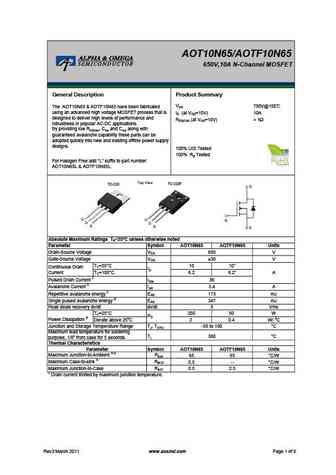
AOT10N65/AOTF10N65 650V,10A N-Channel MOSFET General Description Product Summary VDS 750V@150 The AOT10N65 & AOTF10N65 have been fabricated using an advanced high voltage MOSFET process that is ID (at VGS=10V) 10A designed to deliver high levels of performance and RDS(ON) (at VGS=10V)
0.8. Size:291K sisemi
sif10n65c.pdf 

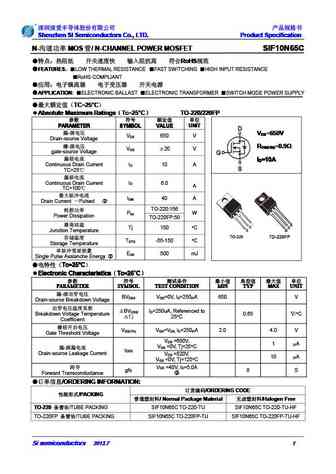
Shenzhen SI Semiconductors Co., LTD. Product Specification Shenzhen SI Semiconductors Co., LTD. Product Specification Shenzhen SI Semiconductors Co., LTD. Product Specification Shenzhen SI Semiconductors Co., LTD. Product Specification N- MOS / N-CHANNEL POWER MOSFET SIF10N65C N- MOS / N-CHANNEL POWER MOSFET SIF10N65C
0.10. Size:991K blue-rocket-elect
brf10n65.pdf 

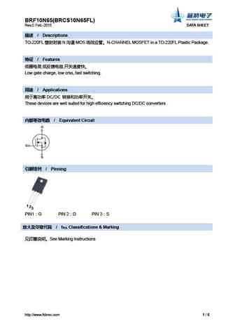
BRF10N65(BRCS10N65FL) Rev.C Feb.-2015 DATA SHEET / Descriptions TO-220FL N MOS N-CHANNEL MOSFET in a TO-220FL Plastic Package. / Features , , Low gate charge, low crss, fast switching. / Applications DC/DC These devices are well suited f
0.12. Size:290K silan
svf10n65cfj.pdf 

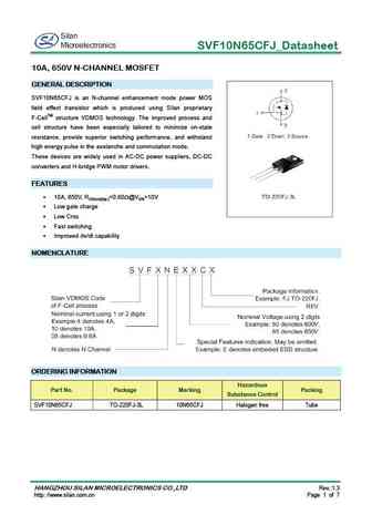
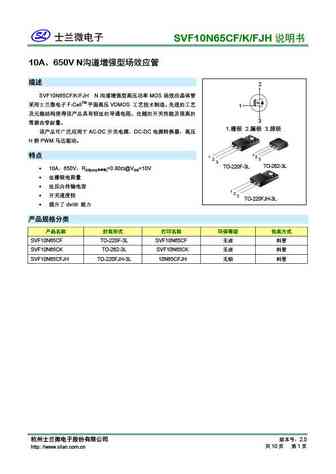
SVF10N65CFJ_Datasheet 10A, 650V N-CHANNEL MOSFET GENERAL DESCRIPTION SVF10N65CFJ is an N-channel enhancement mode power MOS field effect transistor which is produced using Silan proprietary F-CellTM structure VDMOS technology. The improved process and cell structure have been especially tailored to minimize on-state resistance, provide superior switching performance, and withstand
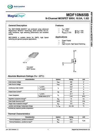
0.15. Size:881K magnachip
mdf10n65bth.pdf 

MDF10N65B N-Channel MOSFET 650V, 10.0A, 1.0 General Description Features The MDF10N65B MOSFET are produced using advanced V = 650V DS MagnaChip s MOSFET Technology, which provides low on- I = 10.0A @ V = 10V D GS state resistance, high switching performance and excellent R 1.0 @ V = 10V DS(ON) GS quality. Applications MDF10N65B is suitable device for
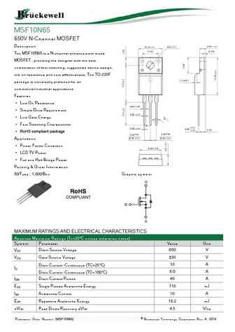
0.16. Size:1078K bruckewell
msf10n65.pdf 

MSF10N65 650V N-Channel MOSFET Description The MSF10N65 is a N-channel enhancement-mode MOSFET , providing the designer with the best combination of fast switching, ruggedized device design, low on-resistance and cost effectiveness. The TO-220F package is universally preferred for all commercial-industrial applications Features Low On Resistance Simple Drive Requir
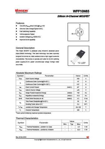
0.17. Size:801K winsemi
wff10n65.pdf 

WFF10N65 WFF10N65 WFF10N65 WFF10N65 Silicon N-Channel MOSFET Silicon N-Channel MOSFET Silicon N-Channel MOSFET Silicon N-Channel MOSFET Features 10A,650V,R (Max 0.95 )@V =10V DS(on) GS Ultra-low Gate Charge(Typical 43nC) Fast Switching Capability 100%Avalanche Tested Isolation Voltage(V =4000V AC) ISO Improved dv/dt capability General Description This
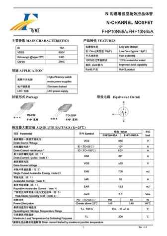
0.18. Size:603K feihonltd
fhp10n65b fhf10n65b.pdf 

N N-CHANNEL MOSFET FHP10N65B/FHF10N65B MAIN CHARACTERISTICS FEATURES Low gate charge ID 10A Crss ( 18pF) Low Crss (typical 18pF ) VDSS 650V Fast switching Rdson-typ 0.75 @Vgs=10V 100% 100% avalanche tested Qg-typ 30nC dv/dt
0.19. Size:543K feihonltd
fhp10n65a fhf10n65a.pdf 

N N-CHANNEL MOSFET FHP10N65A/FHF10N65A MAIN CHARACTERISTICS FEATURES Low gate charge ID 10A Crss ( 18pF) Low Crss (typical 18pF ) VDSS 650V Fast switching Rdson-typ 0.8 @Vgs=10V 100% 100% avalanche tested Qg-typ 29nC dv/dt Improved dv/dt capability RoHS RoHS product APPLICATION High efficiency switch mode pow
0.20. Size:1189K maple semi
slp10n65c slf10n65c.pdf 

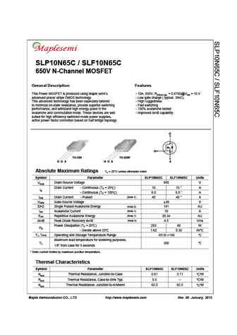
SLP10N65C / SLF10N65C 650V N-Channel MOSFET General Description Features This Power MOSFET is produced using Maple semi s - 10A, 650V, RDS(on) typ. = 0.678 @VGS = 10 V advanced planar stripe DMOS technology. - Low gate charge ( typical 38nC) This advanced technology has been especially tailored - High ruggedness to minimize on-state resistance, provide superior switching - Fast switchi
0.21. Size:666K maple semi
slp10n65s slf10n65s.pdf 

LEAD FREE Pb RoHS SLP10N65S/ SLF10N65S 650V N-Channel MOSFET General Description Features This Power MOSFET is produced using Maple semi s - 10A, 650V, RDS(on) typ=0.8 @VGS = 10 V advanced planar stripe DMOS technology. - Low gate charge ( typical 28.5nC) This advanced technology has been especially tailored - High ruggedness to minimize on-state resistance, provide superior switchi
0.22. Size:2068K maple semi
slf10n65sv.pdf 

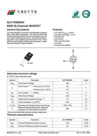
SLF10N65SV 650V N-Channel MOSFET General Description Features This Power MOSFET is produced using Msemitek s advanced 10A*, 650V, RDS(on),typ =0.81 planar stripe DMOS technology. This advanced technology Low gate charge (Qg,typ = 27nC) has been especially tailored to minimize conduction loss, pro- Fast switching vide superior switching performance, and withstand high en-
0.23. Size:978K maple semi
slp10n65a slf10n65a.pdf 

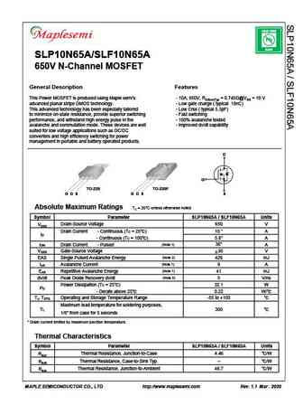
LEAD FREE Pb RoHS SLP10N65A/SLF10N65A 650V N-Channel MOSFET General Description Features This Power MOSFET is produced using Maple semi s - 10A, 650V, RDS(on)Typ = 0.745 @VGS = 10 V advanced planar stripe DMOS technology. - Low gate charge ( typical 19nC) This advanced technology has been especially tailored - Low Crss ( typical 5.3pF) to minimize on-state resistance, provide superi
0.24. Size:1319K samwin
swf10n65d swmn10n65d swy10n65d swp10n65d swu10n65d swj10n65d.pdf 

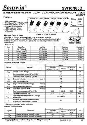
SW10N65D N-channel Enhanced mode TO-220F/TO-220SF/TO-220FT/TO-220/TO-262/TO-262N MOSFET Features TO-262 TO-262N TO-220F TO-220SF TO-220FT TO-220 BVDSS 650V High ruggedness ID 10A Low RDS(ON) (Typ 0.9 )@VGS=10V Low Gate Charge (Typ 35nC) RDS(ON) 0.9 Improved dv/dt Capability 100% Avalanche Tested 2 Application UPS,Inverter, 1 1 1 2 2 1 1 1
0.25. Size:1328K samwin
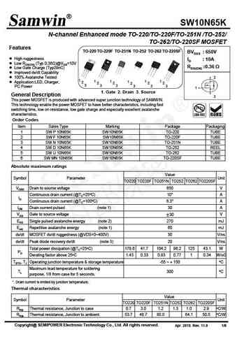
swp10n65k swf10n65k swn10n65k swd10n65k swu10n65k swmn10n65k.pdf 

SW10N65K N-channel Enhanced mode TO-220/TO-220F/TO-251N /TO-252/ TO-262/TO-220SF MOSFET Features TO-220F TO-251N TO-262 TO-220 TO-252 TO-220SF BVDSS 650V High ruggedness ID 10A Low RDS(ON) (Typ 0.36 )@VGS=10V RDS(ON) 0.36 Low Gate Charge (Typ29nC) Improved dv/dt Capability 100% Avalanche Tested 2 1 2 1 2 1 2 1 2 1 2 1 2 Applicatio
0.26. Size:728K samwin
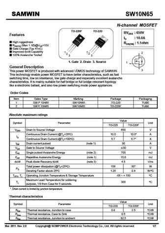
sw10n65 swp10n65 swf10n65.pdf 

SAMWIN SW10N65 N-channel MOSFET TO-220F TO-220 BVDSS 650V Features ID 10.0A High ruggedness RDS(ON) 1.1ohm RDS(ON) (Max 1.1 )@VGS=10V Gate Charge (Typ 47nC) Improved dv/dt Capability 1 1 2 2 2 100% Avalanche Tested 3 3 1. Gate 2. Drain 3. Source 1 General Description 3 This power MOSFET is produced with advanced VDMOS technology of SAMWIN. This
0.27. Size:952K samwin
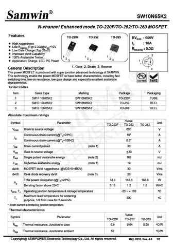
swf10n65k2 swd10n65k2 swb10n65k2.pdf 

SW10N65K2 N-channel Enhanced mode TO-220F/TO-252/TO-263 MOSFET Features TO-220F TO-252 TO-263 BVDSS 650V High ruggedness ID 10A Low RDS(ON) (Typ 0.3 )@VGS=10V RDS(ON) 0.3 Low Gate Charge (Typ 21nC) Improved dv/dt Capability 2 1 1 1 100% Avalanche Tested 2 2 2 3 3 3 1 Application Charge, LED, PC Power 1. Gate 2. Drain 3. Sou
0.28. Size:577K trinnotech
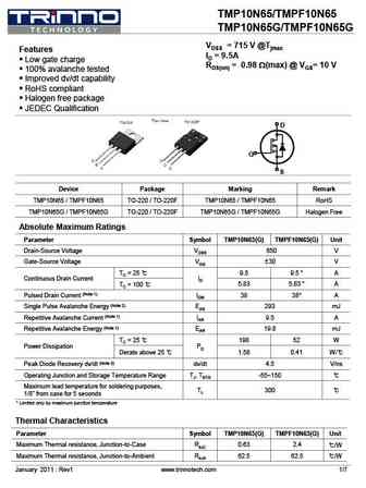
tmp10n65 tmpf10n65.pdf 

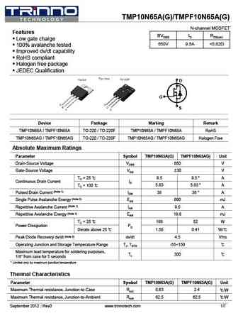
TMP10N65/TMPF10N65 TMP10N65G/TMPF10N65G VDSS = 715 V @Tjmax Features ID = 9.5A Low gate charge RDS(on) = 0.98 W(max) @ VGS= 10 V 100% avalanche tested Improved dv/dt capability RoHS compliant Halogen free package JEDEC Qualification D G S Device Package Marking Remark TMP10N65 / TMPF10N65 TO-220 / TO-220F TMP10N65 / TMPF10N65 RoHS TMP10N
0.29. Size:607K trinnotech
tmp10n65a tmpf10n65a.pdf 

TMP10N65A(G)/TMPF10N65A(G) N-channel MOSFET Features BVDSS ID RDS(on) Low gate charge 650V 9.5A
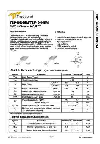
0.30. Size:1254K truesemi
tsp10n65m tsf10n65m.pdf 

TSP10N65M/TSF10N65M 650V N-Channel MOSFET General Description Features This Power MOSFET is produced using Truesemi s 10.0A,650V,Max.RDS(on)=1.0 @ VGS =10V advanced planar stripe DMOS technology. This advanced technology has been especially tailored to Low gate charge(typical 48nC) minimize on-state resistance, provide superior switching High ruggedness performance, a
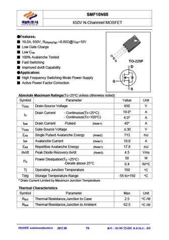
0.32. Size:901K huake
smf10n65.pdf 

SMF10N65 650V N-Channnel MOSFET Features 10.0A, 650V, R =0.80 @V =10V DS(on)(Typ) GS Low Gate Charge Low C rss 100% Avalanche Tested Fast Switching Improved dv/dt Capability Application High Frequency Switching Mode Power Supply Active Power Factor Correction Absolute Maximum Ratings(Tc=25 C unless otherwise noted) Symbol Parameter Va
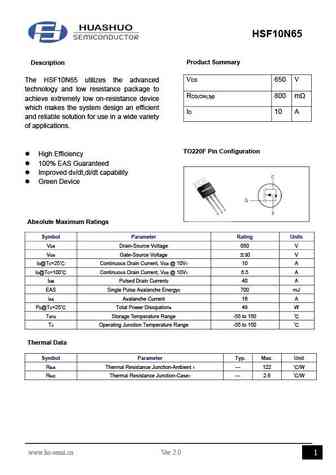
0.33. Size:1531K huashuo
hsf10n65.pdf 

HSF10N65 Product Summary Description VDS 650 V The HSF10N65 utilizes the advanced technology and low resistance package to RDS(ON),typ 800 m achieve extremely low on-resistance device which makes the system design an efficient ID 10 A and reliable solution for use in a wide variety of applications. TO220F Pin Configuration High Efficiency 100% EAS Guarante
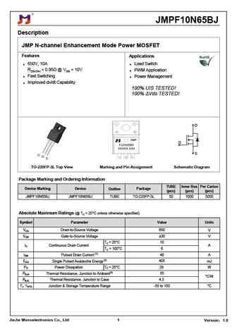
0.34. Size:491K jiejie micro
jmpf10n65bj.pdf 

JMPF10N65BJ Description JMP N-channel Enhancement Mode Power MOSFET Features Applications 650V, 10A Load Switch RDS(ON)
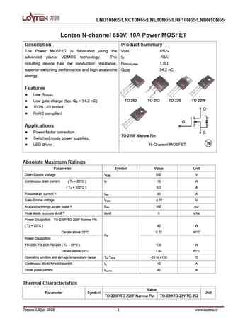
0.35. Size:1293K lonten
lnd10n65 lnc10n65 lne10n65 lnf10n65 lndn10n65.pdf 

LND10N65/LNC10N65/LNE10N65/LNF10N65/LNDN10N65 Lonten N-channel 650V, 10A Power MOSFET Description Product Summary The Power MOSFET is fabricated using the V 650V DSS advanced planer VDMOS technology. The I 10A D resulting device has low conduction resistance, R 1.0 DS(on),max superior switching performance and high avalanche Q 34.2 nC g,typ energy. Features Low R DS(on)
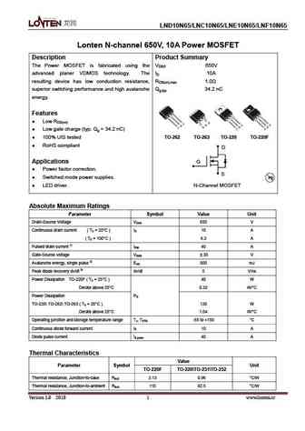
0.36. Size:1051K lonten
lnd10n65 lnc10n65 lne10n65 lnf10n65.pdf 

LND10N65/LNC10N65/LNE10N65/LNF10N65 Lonten N-channel 650V, 10A Power MOSFET Description Product Summary The Power MOSFET is fabricated using the VDSS 650V advanced planer VDMOS technology. The ID 10A resulting device has low conduction resistance, RDS(on),max 1.0 superior switching performance and high avalanche Qg,typ 34.2 nC energy. Features Low RDS(on) Low gate
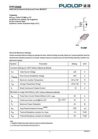
0.37. Size:6851K cn puolop
ptf10n65.pdf 

PTF1 0N65 65 0V/1 0A N-Channel A dv anced Power MOSFET Features RDS(on) (Typical 0.6 )@VGS=10V Improved dv/dt Capability, High Ruggedness 100% Avalanche Tested Maximum Junction Temperature Range (150 C) G D S TO-220F Absolute Maximum Ratings Stresses exceeding Maximum Ratings may damage the device. Maximum Ratings are stress ratings only. Functional operation above
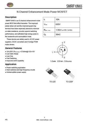
0.38. Size:1202K cn sps
smirf10n65.pdf 

SMIRF10N65 30V /36A Single N Power MOSFET N-Channel Enhancement Mode Power MOSFET Description ID 10A SMIRF10N65 is an N-channel enhancement mode power MOS field effect transistor. The improved VDSS 650V planar stripe cell and the improved guard ring terminal have been especially tailored to minimize Rdson max 1.0 (VGS=10V, ID=5A) on-state resistance, provide superior
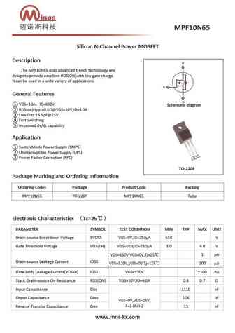
0.39. Size:461K cn minos
mpf10n65.pdf 

Silicon N-Channel Power MOSFET Description The MPF10N65 uses advanced trench technology and design to provide excellent RDS(ON)with low gate charge. It can be used in a wide variety of applications. General Features VDS=10A ID=650V Schematic diagram RDS(on)(typ)=0.6 @VGS=10V,ID=4.0A Low Crss 18.5pF@25V Fast switching Improved dv/dt capability Application
0.40. Size:255K inchange semiconductor
aotf10n65.pdf 
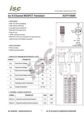
isc N-Channel MOSFET Transistor AOTF10N65 FEATURES With TO-220F packaging High speed switching Low gate input resistance Standard level gate drive Easy to use 100% avalanche tested Minimum Lot-to-Lot variations for robust device performance and reliable operation APPLICATIONS Power supply Switching applications ABSOLUTE MAXIMUM RATINGS(T =25 ) a SYMBOL P
Otros transistores... LPN1010C
, LPN2010C
, 2N7002KS6
, SR3400
, SR3401
, SRX3134K
, D2N65
, D4N65
, RFP50N06
, F12N65
, .8205A
, .8205S
, .8205P
, 2060K.
, 2301P
, 2302P
, 3050K
.
History: NTD4909N
| AOK22N50L
