3407 MOSFET Equivalente. Reemplazo. Hoja de especificaciones. Principales características
Número de Parte: 3407
Tipo de FET: MOSFET
Polaridad de transistor: P
ESPECIFICACIONES MÁXIMAS
Pdⓘ - Máxima disipación de potencia: 0.35 W
|Vds|ⓘ - Voltaje máximo drenador-fuente: 30 V
|Vgs|ⓘ - Voltaje máximo fuente-puerta: 20 V
|Id|ⓘ - Corriente continua de drenaje: 4.1 A
Tjⓘ - Temperatura máxima de unión: 150 °C
CARACTERÍSTICAS ELÉCTRICAS
trⓘ - Tiempo de subida: 5 nS
Cossⓘ - Capacitancia de salida: 120 pF
RDSonⓘ - Resistencia estado encendido drenaje a fuente: 0.06 Ohm
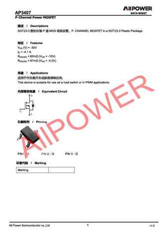
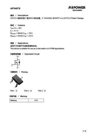
Encapsulados: SOT23
Búsqueda de reemplazo de 3407 MOSFET
- Selecciónⓘ de transistores por parámetros
3407 datasheet
3407.pdf
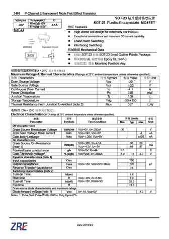
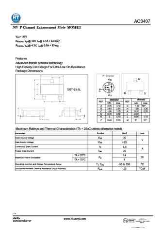
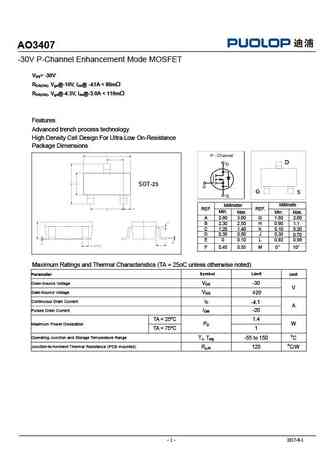
3407 P-Channel Enhancement Mode Field Effect Transistor SOT-23 V(BR)DSS RDS(ON)MAX ID SOT-23 Plastic-Encapsulate MOSFET 60m @-10V -30V -4.1A 87m @-4.5V Features SOT-23 High dense cell design for extremely low RDS(on). Exceptional on-resistance and maximum DC current capability. Load/Power Switching. Interfacing Switching
ao3407 a7 a79t x7kv code psot23.pdf
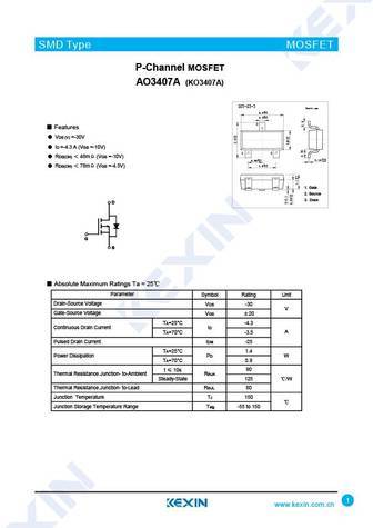
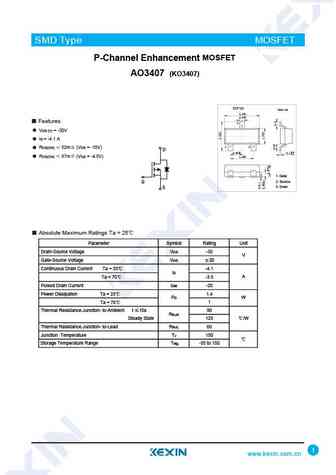
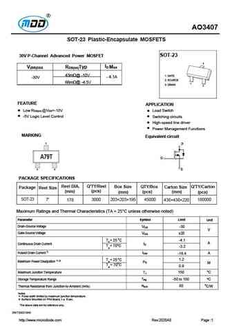
SMD Type MOSFET P-Channel MOSFET AO3407A (KO3407A) SOT-23-3 Unit mm +0.2 2.9 -0.1 +0.1 0.4 -0.1 3 Features VDS (V) =-30V ID =-4.3 A (VGS =-10V) 1 2 RDS(ON) 48m (VGS =-10V) +0.02 +0.1 0.15 -0.02 0.95-0.1 +0.1 1.9-0.2 RDS(ON) 78m (VGS =-4.5V) 1. Gate 2. Source 3. Drain D D G G S S Absolute Maximum Ratings Ta = 25 Paramete
irfb3407zpbf.pdf
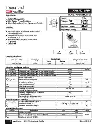
IRFB3407ZPbF HEXFET Power MOSFET Applications VDSS 75V D l Battery Management RDS(on) typ. 5.0m l High Speed Power Switching l Hard Switched and High Frequency Circuits max. 6.4m G ID (Silicon Limited) 122A S Benefits ID (Package Limited) 120A l Improved Gate, Avalanche and Dynamic dv/dt Ruggedness D l Fully Characterized Capacitance and Avalanche SOA l Enhanced b
2sk3407.pdf
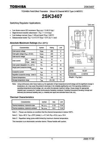
2SK3407 TOSHIBA Field Effect Transistor Silicon N Channel MOS Type ( -MOSV) 2SK3407 Switching Regulator Applications Unit mm Low drain-source ON resistance RDS (ON) = 0.48 (typ.) High forward transfer admittance Yfs = 7.5 S (typ.) Low leakage current IDSS = 100 A (max) (VDS = 450 V) Enhancement-mode Vth = 2.4 3.4 V (VDS = 10 V, ID = 1 mA) Absolute
cph3407.pdf
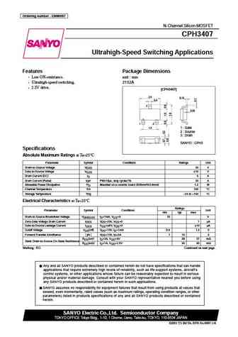
Ordering number ENN6997 CPH3407 N-Channel Silicon MOSFET CPH3407 Ultrahigh-Speed Switching Applications Features Package Dimensions Low ON-resistance. unit mm Ultrahigh-speed switching. 2152A 2.5V drive. [CPH3407] 2.9 0.15 0.4 3 0.05 1 2 1.9 1 Gate 2 Source 3 Drain SANYO CPH3 Specifications Absolute Maximum Ratings at Ta=25 C Parameter Symbol Condi
si3407dv.pdf
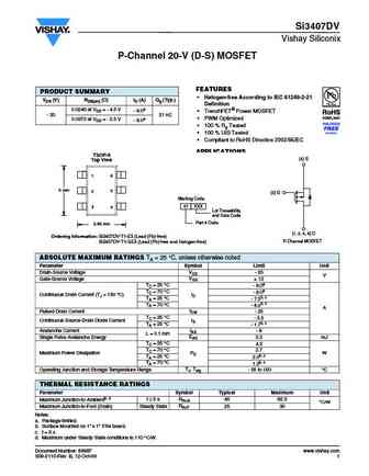
Si3407DV Vishay Siliconix P-Channel 20-V (D-S) MOSFET FEATURES PRODUCT SUMMARY Halogen-free According to IEC 61249-2-21 VDS (V) RDS(on) ( )ID (A) Qg (Typ.) Definition 0.0240 at VGS = - 4.5 V - 8.0a TrenchFET Power MOSFET - 20 21 nC PWM Optimized 0.0372 at VGS = - 2.5 V - 8.0a 100 % Rg Tested 100 % UIS Tested Compliant to RoHS Directive 2002/9
si3407.pdf
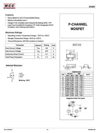
SI3407 Features Epoxy Meets UL 94 V-0 Flammability Rating Moisture Sensitivity Level 1 Halogen Free Available Upon Request By Adding Suffix "-HF" P-CHANNEL Lead Free Finish/RoHS Compliant ("P" Suffix Designates RoHS Compliant. See Ordering Information) MOSFET Maximum Ratings Operating Junction Temperature Range -55 C to +150 C Storage Temperature Range -5
smg3407.pdf
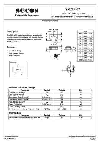
SMG3407 -4.1A, -30V,RDS(ON) 52m Elektronische Bauelemente P-Channel Enhancement Mode Power Mos.FET RoHS Compliant Product A SC-59 Description L Dim Min Max The SMG3407 uses advanced trench technology to 3 A 2.70 3.10 S B Top View provide excellent on-resistance with low gate change. 2 1 B 1.40 1.60 The device is suitable for use as a load switch or in C 1.00 1.30 PWM
cj3407.pdf
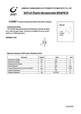
JIANGSU CHANGJIANG ELECTRONICS TECHNOLOGY CO., LTD SOT-23 Plastic-Encapsulate MOSFETS CJ3407 P-Channel Enhancement Mode Field Effect Transistor SOT-23 General Description The CJ3407 uses advanced trench technology to provide excellent RDS(on) with low gate charge. This device is suitable for use as a load 1. GATE switch or in PWM applications. 2. SOURCE 3. DRAIN MARKING 3
cjl3407.pdf
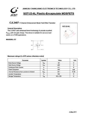
JIANGSU CHANGJIANG ELECTRONICS TECHNOLOGY CO., LTD SOT-23-6L Plastic-Encapsulate MOSFETS CJL3407 P-Channel Enhancement Mode Field Effect Transistor SOT-23-6L General Description The CJ3407 uses advanced trench technology to provide excellent RDS(on) with low gate charge. This device is suitable for use as a load switch or in PWM applications. MARKING R7 Maximum rati
cjk3407.pdf
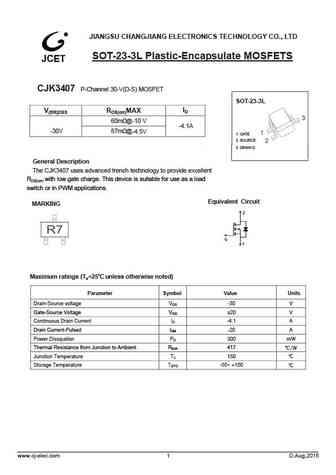
JIANGSU CHANGJIANG ELECTRONICS TECHNOLOGY CO., LTD SOT-23-3L Plastic-Encapsulate MOSFETS CJK34 07 P-Channel 30-V(D-S) MOSFET SOT-23-3L ID V(BR)DSS RDS(on)MAX 60m @-10 V -4.1A -30V 87m @-4.5V 1. GATE 2. SOURCE 3. DRAIN D General Description The CJK3407 uses advanced trench technology to provide excellent RDS(on) with low gate charge. This device is suitable for
ao3407.pdf
AO3407 30V P-Channel Enhancement Mode MOSFET V = -30V DS R , V DS(ON) gs@-10V, I 4.1A
cem3407l.pdf
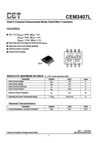
CEM3407L Dual P-Channel Enhancement Mode Field Effect Transistor FEATURES -30V, -5.1A, RDS(ON) = 48m @VGS = -10V. RDS(ON) = 65m @VGS = -4.5V. RDS(ON) = 115m @VGS = -2.5V. Super high dense cell design for extremely low RDS(ON). High power and current handing capability. Lead free product is acquired. D1 D1 D2 D2 8 7 6 5 Surface mount Package. SO-8 1 2 3 4 1 S1 G1 S2 G2
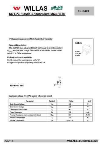
se3407.pdf
FM120-M WILLAS THRU SE3407 SOT-23 Plastic-Encapsulate MOSFETS FM1200-M 1.0A SURFACE MOUNT SCHOTTKY BARRIER RECTIFIERS -20V- 200V SOD-123 PACKAGE Pb Free Produ Package outline Features Batch process design, excellent power dissipation offers better reverse leakage current and thermal resistance. SOD-123H Low profile surface mounted application in order to optimize b
wpm3407.pdf
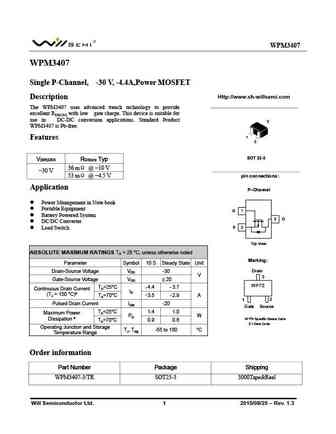
WPM3407 WPM3407 Single P-Channel, -30 V, -4.4A,Power MOSFET Http //www.sh-willsemi.com Description The WPM3407 uses advanced trench technology to provide excellent RDS(ON) with low gate charge. This device is suitable for use in DC-DC conversion applications. Standard Product 3 WPM3407 is Pb-free. 1 Features 2 SOT 23-3 V R Typ (BR)DSS DS(on) 36 m @ -10 V -30 V 53 m @ -4.5
ao3407.pdf
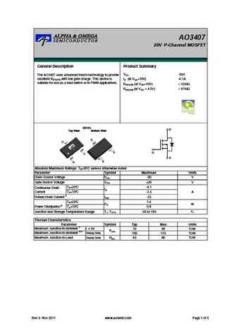
AO3407 30V P-Channel MOSFET General Description Product Summary VDS -30V The AO3407 uses advanced trench technology to provide excellent RDS(ON) with low gate charge. This device is ID (at VGS=10V) -4.1A suitable for use as a load switch or in PWM applications. RDS(ON) (at VGS=10V)
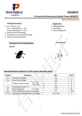
ao3407a.pdf
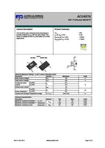
AO3407A 30V P-Channel MOSFET General Description Product Summary VDS -30V The AO3407A uses advanced trench technology to provide excellent RDS(ON) with low gate charge. This ID (at VGS=-10V) -4.3A device is suitable for use as a load switch or in PWM RDS(ON) (at VGS=-10V)
am3407pe.pdf
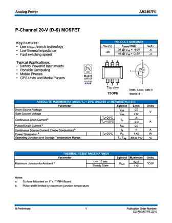
Analog Power AM3407PE P-Channel 20-V (D-S) MOSFET PRODUCT SUMMARY Key Features rDS(on) (m ) VDS (V) ID(A) Low r trench technology DS(on) 34 @ VGS = -4.5V -5 Low thermal impedance -20 48 @ VGS = -2.5V -3 Fast switching speed Typical Applications Battery Powered Instruments Portable Computing Mobile Phones GPS Units and Media Players Drain 1,2,5,6
afp3407as.pdf
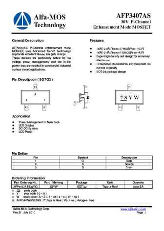
AFP3407AS Alfa-MOS 30V P-Channel Technology Enhancement Mode MOSFET General Description Features AFP3407AS, P-Channel enhancement mode -30V/-2.8A,RDS(ON)=77m @VGS=-10.0V MOSFET, uses Advanced Trench Technology -30V/-2.4A,RDS(ON)=102m @VGS=-4.5V to provide excellent RDS(ON), low gate charge. Super high density cell design for extremely These devices are particularl
afp3407s.pdf
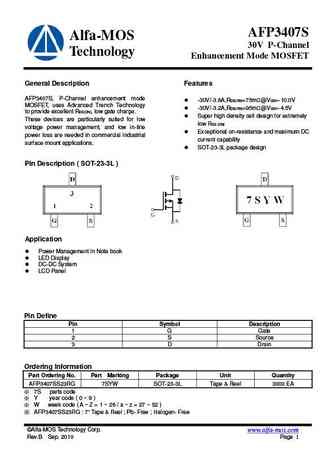
AFP3407S Alfa-MOS 30V P-Channel Technology Enhancement Mode MOSFET General Description Features AFP3407S, P-Channel enhancement mode -30V/-3.6A,RDS(ON)=75m @VGS=-10.0V MOSFET, uses Advanced Trench Technology -30V/-3.2A,RDS(ON)=95m @VGS=-4.5V to provide excellent RDS(ON), low gate charge. Super high density cell design for extremely These devices are particularly s
ao3407.pdf
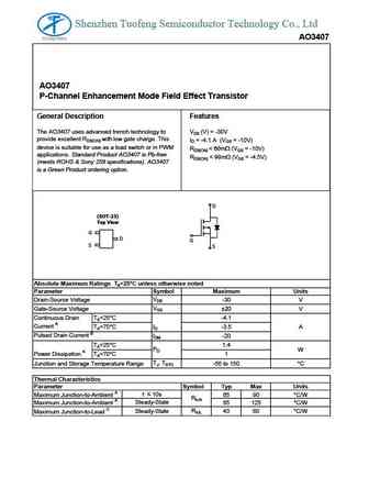
Shenzhen Tuofeng Semiconductor Technology Co., Ltd AO3407 AO3407 P-Channel Enhancement Mode Field Effect Transistor General Description Features The AO3407 uses advanced trench technology to VDS (V) = -30V provide excellent RDS(ON) with low gate charge. This ID = -4.1 A (VGS = -10V) device is suitable for use as a load switch or in PWM RDS(ON)
yw3407 fg.pdf
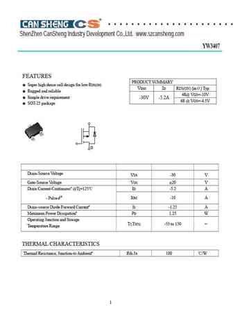
ShenZhen CanSheng Industry Development Co.,Ltd. www.szcansheng.com YW3407 FEATURES PRODUCT SUMMARY Super high dense cell design for low RDS(ON) RDS(ON) (m ) Typ VDSS ID Rugged and reliable 48@ VGS=-10V Simple drive requirement -30V -5.2A 68 @ VGS=-4.5V SOT-23 package D Drain-Source Voltage VDS -30 V Gate-Sourc
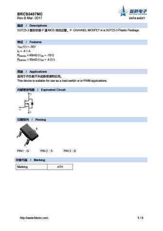
brcs3407mc.pdf
BRCS3407MC Rev.B Mar.-2017 DATA SHEET / Descriptions SOT23-3 P MOS P- CHANNEL MOSFET in a SOT23-3 Plastic Package. / Features VDS (V) = -30V ID = -4.1 A RDS(ON)
lp3407lt1g.pdf
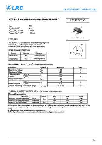
LESHAN RADIO COMPANY, LTD. 30V P-Channel Enhancement-Mode MOSFET LP3407LT1G VDS -30V 3 ID (VGS = -10V) -4.1A RDS(ON) (VGS = -10V)
lp3407lt1g s-lp3407lt1g.pdf
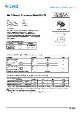
LESHAN RADIO COMPANY, LTD. LP3407LT1G 30V P-Channel Enhancement-Mode MOSFET S-LP3407LT1G VDS -30V 3 ID (VGS = -10V) -4.1A RDS(ON) (VGS = -10V)
sm3407psqa.pdf
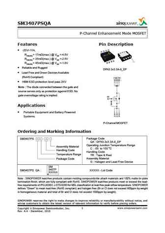
SM3407PSQA P-Channel Enhancement Mode MOSFET Features Pin Description D -20V/-11A, D D D RDS(ON) = 17m (max.) @ VGS =-4.5V RDS(ON) = 25m (max.) @ VGS =-2.5V G S S RDS(ON) = 45m (max.) @ VGS =-1.8V S Reliable and Rugged DFN3.3x3.3A-8_EP Lead Free and Green Devices Available (RoHS Compliant) ( 5,6,7,8 ) DDDD HBM ESD protection level pass 2KV Note The diode connected
wpm3407.pdf
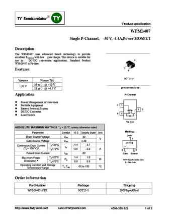
Product specification WPM3407 Single P-Channel, -30 V, -4.4A,Power MOSFET Description The WPM3407 uses advanced trench technology to provide excellent RDS(ON) with low gate charge. This device is suitable for 3 use in DC-DC conversion applications. Standard Product WPM3407 is Pb-free. 1 Features 2 SOT 23-3 V R Typ (BR)DSS DS(on) 36 m @ -10 V -30 V pin connections 53 m
dmg3407ssn.pdf
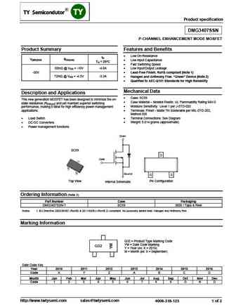
Product specification DMG3407SSN P-CHANNEL ENHANCEMENT MODE MOSFET Product Summary Features and Benefits Low On-Resistance ID V(BR)DSS RDS(ON) Low Input Capacitance TA = 25 C Fast Switching Speed 50m @ VGS = -10V -4.0A Low Input/Output Leakage -30V Lead-Free Finish; RoHS compliant (Note 1) 72m @ VGS = -4.5V -3.3A Halogen and Antimony Free.
ftk3407l.pdf
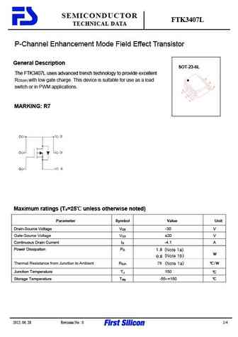
SEMICONDUCTOR FTK3407L TECHNICAL DATA P-Channel Enhancement Mode Field Effect Transistor General Description SOT-23-6L The FTK3407L uses advanced trench technology to provide excellent RDS(on) with low gate charge. This device is suitable for use as a load switch or in PWM applications. MARKING R7 Maximum ratings (Ta=25 unless otherwise noted) Parameter Symbol Value Unit
ftk3407.pdf
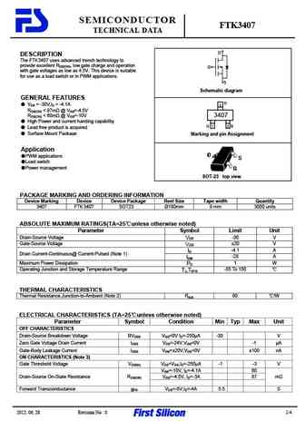
SEMICONDUCTOR FTK3407 TECHNICAL DATA D DESCRIPTION The FTK3407 uses advanced trench technology to provide excellent RDS(ON), low gate charge and operation G with gate voltages as low as 4.5V. This device is suitable for use as a load switch or in PWM applications. S Schematic diagram GENERAL FEATURES D VDS = -30V,ID = -4.1A 3 RDS(ON)
ao3407.pdf
SMD Type IC SMD Type MOSFET P-Channel Enhancement MOSFET AO3407 (KO3407) SOT-23 Unit mm +0.1 2.9 -0.1 +0.1 0.4 -0.1 Features 3 VDS (V) = -30V ID = -4.1 A 1 2 RDS(ON) 52m (VGS = -10V) D +0.1 +0.05 0.95 -0.1 0.1 -0.01 +0.1 RDS(ON) 87m (VGS = -4.5V) 1.9 -0.1 1.Base 1. Gate 2.Emitter 2. Source G 3. Drain 3.collector S Absolute Maximum Ratings Ta = 25 Parameter Sy
ao3407 ko3407.pdf

SMD Type IC SMD Type MOSFET P-Channel Enhancement MOSFET AO3407 (KO3407) SOT-23-3 Unit mm +0.2 2.9-0.1 +0.1 0.4 -0.1 3 Features VDS (V) = -30V ID = -4.1 A 1 2 +0.02 +0.1 0.15 -0.02 RDS(ON) 52m (VGS = -10V) 0.95 -0.1 D 1.9+0.1 -0.2 RDS(ON) 87m (VGS = -4.5V) 1. Gate 2. Source G 3. Drain S Absolute Maximum Ratings Ta = 25 Parameter Symbol Rating Unit Drain-Sourc
ko3407.pdf
SMD Type IC SMD Type Transistors P-Channel Enhancement Mode Field Effect Transistor KO3407 SOT-23 Unit mm +0.1 2.9-0.1 +0.1 0.4-0.1 Features 3 VDS (V) = -30V ID =-4.1 A 12 RDS(ON) 52m (VGS = -10V) +0.1 +0.05 0.95-0.1 0.1-0.01 +0.1 RDS(ON) 87m (VGS = -4.5V) 1.9-0.1 1.Base 1. Gate 2.Emitter 2. Source 3. Drain 3.collector Absolute Maximum Ratings Ta = 25 Parameter Symb
ao3407a-3.pdf

SMD Type MOSFET P-Channel MOSFET AO3407A (KO3407A) SOT-23-3 Unit mm +0.2 2.9 -0.1 +0.1 0.4 -0.1 3 Features VDS (V) =-30V ID =-4.3 A (VGS =-10V) 1 2 RDS(ON) 48m (VGS =-10V) +0.02 +0.1 0.15 -0.02 0.95-0.1 +0.1 1.9-0.2 RDS(ON) 78m (VGS =-4.5V) 1. Gate 2. Source 3. Drain D D G G S S Absolute Maximum Ratings Ta = 25 Paramete
ao3407a.pdf
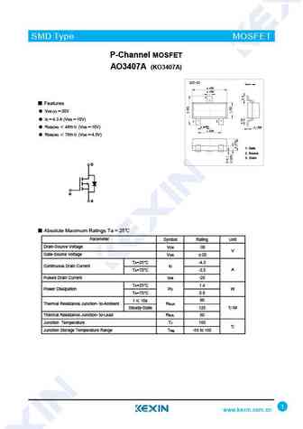
SMD Type MOSFET P-Channel MOSFET AO3407A (KO3407A) SOT-23 Unit mm 2.9+0.1 -0.1 +0.1 0.4-0.1 3 Features VDS (V) =-30V ID =-4.3 A (VGS =-10V) 1 2 +0.1 +0.05 0.95 -0.1 RDS(ON) 48m (VGS =-10V) 0.1 -0.01 +0.1 1.9 -0.1 RDS(ON) 78m (VGS =-4.5V) 1. Gate 2. Source 3. Drain D D G G S S Absolute Maximum Ratings Ta = 25 Parameter Sy
ao3407hf.pdf
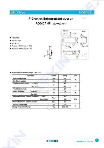
SMD Type IC SMD Type MOSFET P-Channel Enhancement MOSFET AO3407 HF (KO3407 HF) SOT-23-3 Unit mm +0.2 2.9-0.1 +0.1 0.4 -0.1 3 Features VDS (V) = -30V ID = -4.1 A 1 2 +0.02 +0.1 0.15 -0.02 RDS(ON) 52m (VGS = -10V) 0.95 -0.1 D 1.9+0.1 -0.2 RDS(ON) 87m (VGS = -4.5V) 1. Gate 2. Source G 3. Drain S Absolute Maximum Ratings Ta = 25 Parameter Symbol Rating Unit Drain-
ao3407-3.pdf
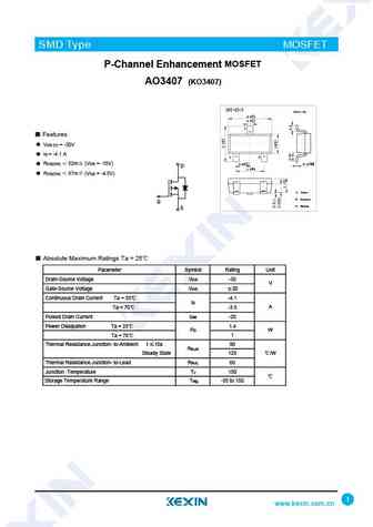
SMD Type IC SMD Type MOSFET P-Channel Enhancement MOSFET AO3407 (KO3407) SOT-23-3 Unit mm +0.2 2.9-0.1 +0.1 0.4 -0.1 3 Features VDS (V) = -30V ID = -4.1 A 1 2 +0.02 +0.1 0.15 -0.02 RDS(ON) 52m (VGS = -10V) 0.95 -0.1 D 1.9+0.1 -0.2 RDS(ON) 87m (VGS = -4.5V) 1. Gate 2. Source G 3. Drain S Absolute Maximum Ratings Ta = 25 Parameter Symbol Rating Unit Drain-Sourc
pja3407.pdf
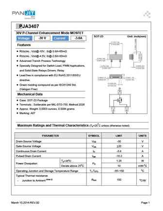
PPJA3407 30V P-Channel Enhancement Mode MOSFET SOT-23 Unit inch(mm) Voltage -30 V Current -3.8A Features RDS(ON) , VGS@-10V, ID@-3.8A
am3407.pdf
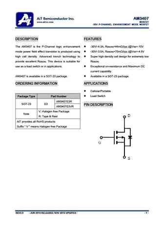
AiT Semiconductor Inc. AM3407 www.ait-ic.com MOSFET -30V P-CHANNEL ENHANCEMENT MODE MOSFET DESCRIPTION FEATURES The AM3407 is the P-Channel logic enhancement -30V/-4.3A, R =44m (typ.)@V =-10V DS(ON) GS mode power field effect transistor is produced using -30V/-3.0A, R =70m (typ.)@V =-4.5V DS(ON) GS high cell density. Advanced trench technology to Super high density c
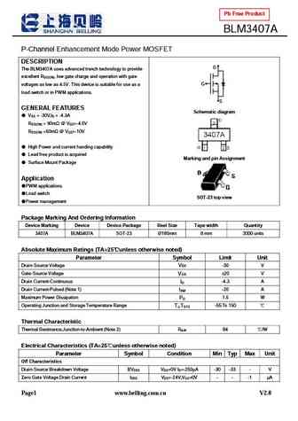
blm3407.pdf
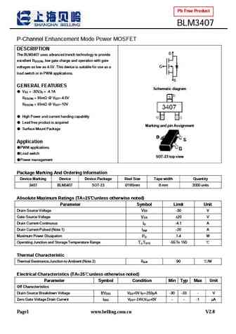
Pb Free Product BLM3407 P-Channel Enhancement Mode Power MOSFET DESCRIPTION D The BLM3407 uses advanced trench technology to provide excellent R , low gate charge and operation with gate DS(ON) G voltages as low as 4.5V. This device is suitable for use as a load switch or in PWM applications. S GENERAL FEATURES Schematic diagram V = -30V,I = -4.1A DS D R
elm33407ca.pdf
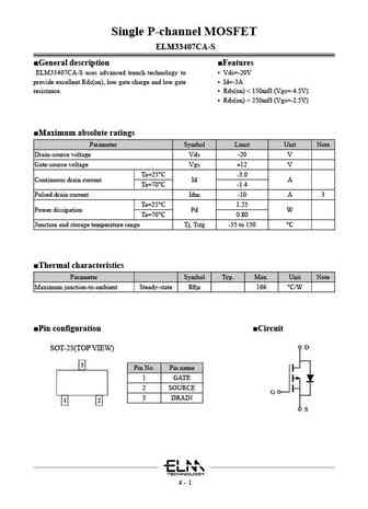
Single P-channel MOSFET ELM33407CA-S General description Features ELM33407CA-S uses advanced trench technology to Vds=-20V provide excellent Rds(on), low gate charge and low gate Id=-3A resistance. Rds(on)
elm13407ca-s.pdf
Single P-channel MOSFET ELM13407CA-S General description Features ELM13407CA-S uses advanced trench technology to Vds=-30V provide excellent Rds(on), low gate charge and low gate Id=-4.1A (Vgs=-10V) resistance. Rds(on)
gsm3407s.pdf
GSM3407S 30V P-Channel Enhancement Mode MOSFET Product Description Features GSM3407S, P-Channel enhancement mode -30V/-3.6A,RDS(ON)=75m @VGS=-10V MOSFET, uses Advanced Trench Technology to -30V/-3.2A,RDS(ON)=95m @VGS=-4.5V provide excellent RDS(ON), low gate charge. Super high density cell design for extremely low RDS (ON) These devices are particularly suited for
gsm3407as.pdf
30V P-Channel Enhancement Mode MOSFET Product Description Features GSM3407AS, P-Channel enhancement mode -30V/-2.8A,RDS(ON)=77m @VGS=-10.0V MOSFET, uses Advanced Trench Technology to -30V/-2.4A,RDS(ON)=102m @VGS=-4.5V provide excellent RDS(ON), low gate charge. Super high density cell design for extremely These devices are particularly suited for low low RDS (ON)
kia3407.pdf
-4.1A -30V 3407 P-CHANNELMOSFET KIA KIA KIA SEMICONDUCTORS SEMICONDUCTORS SEMICONDUCTORS 1.Description The KIA3407 uses advanced trench technology to provide excellent R ,low gate DS(on) charge.This device is suitable for use as a load switch or in PWMapplications.Standard Product KIA3407 is Pb-free(meets ROHS&Sony 259 specifications).KIA3407 is a Green Product ordering option.
ao3407g.pdf
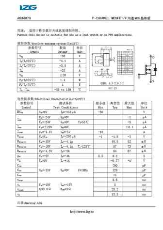
AO3407G P-CHANNEL MOSFET/P MOS Purpose This device is suitable for use as a load switch or in PWM applications. /Absolute maximum ratings(Ta=25 ) Symbol Rating Unit V -30 V DS I (T =25 ) -4.1 A D a I (T =70 ) -3.5 A D a I -20 A DM V 20 V GS P (
nce3407a.pdf
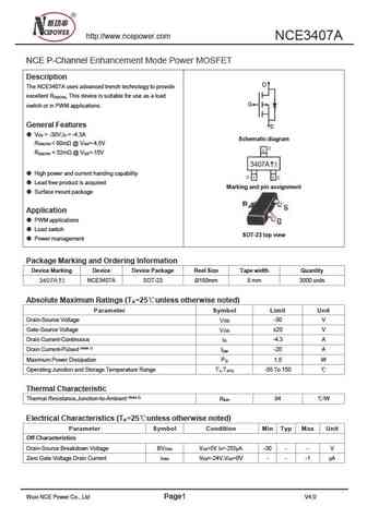
http //www.ncepower.com NCE3407A NCE P-Channel Enhancement Mode Power MOSFET Description D The NCE3407A uses advanced trench technology to provide excellent R , This device is suitable for use as a load DS(ON) G switch or in PWM applications. General Features S V = -30V,I = -4.3A DS D Schematic diagram R
nce3407.pdf
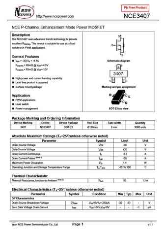
Pb Free Product http //www.ncepower.com NCE3407 NCE P-Channel Enhancement Mode Power MOSFET Description D The NCE3407 uses advanced trench technology to provide excellent RDS(ON), This device is suitable for use as a load G switch or in PWM applications. S General Features VDS = -30V,ID = -4.1A Schematic diagram RDS(ON)
nce3407ay.pdf
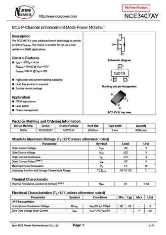
Pb Free Product http //www.ncepower.com NCE3407AY NCE P-Channel Enhancement Mode Power MOSFET D Description The NCE3407AY uses advanced trench technology to provide G excellent RDS(ON), This device is suitable for use as a load switch or in PWM applications. S General Features Schematic diagram VDS = -30V,ID = -4.3A RDS(ON)
nce3407e.pdf
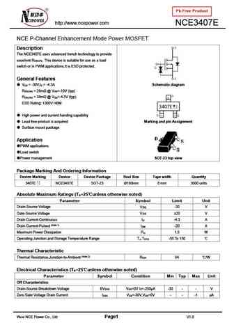
Pb Free Product http //www.ncepower.com NCE3407E NCE P-Channel Enhancement Mode Power MOSFET Description The NCE3407E uses advanced trench technology to provide excellent R . This device is suitable for use as a load DS(ON) switch or in PWM applications.It is ESD protected. General Features V = -30V,I = -4.3A Schematic diagram DS D R = 28m @ V =-10V (typ) DS(ON) GS R = 38m
smc3407.pdf
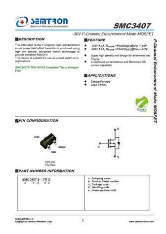
SMC3407 -30V P-Channel Enhancement Mode MOSFET DESCRIPTION FEATURE The SMC3407 is the P-Channel logic enhancement -30V/-4.3A, RDS(ON) =44m (typ.)@VGS =-10V mode power field effect transistor is produced using -30V/-3.0A, RDS(ON) =70m (typ.)@VGS =-4.5V high cell density. advanced trench technology to provide excellent RDS(ON) Super high density cell design
stp3407.pdf
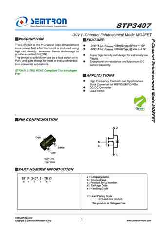
STP3407 -30V P-Channel Enhancement Mode MOSFET DESCRIPTION FEATURE The STP3407 is the P-Channel logic enhancement -30V/-4.3A, RDS(ON) =38m (typ.)@VGS =-10V mode power field effect transistor is produced using -30V/-3.0A, RDS(ON) =58m (typ.)@VGS =-4.5V high cell density. advanced trench technology to provide excellent RDS(ON). Super high density cell desig
sl3407.pdf
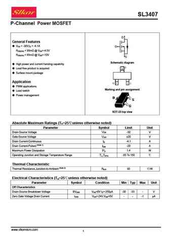
SL3407 P-Channel Power MOSFET D General Features VDS = -30V,ID = -4.1A G RDS(ON)
st3407srg.pdf
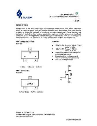
ST3407SRG P Channel Enhancement Mode MOSFET -3.6A DESCRIPTION ST3407SRG is the P-Channel logic enhancement mode power field effect transistor which is produced using high cell density, DMOS trench technology. This high density process is especially tailored to minimize on-state resistance. These devices are particularly suited for low voltage application such as cellular phone a
st3407s23rg.pdf
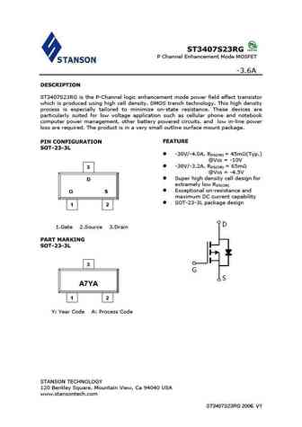
ST3407S23RG P Channel Enhancement Mode MOSFET -3.6A DESCRIPTION ST3407S23RG is the P-Channel logic enhancement mode power field effect transistor which is produced using high cell density, DMOS trench technology. This high density process is especially tailored to minimize on-state resistance. These devices are particularly suited for low voltage application such as cellular pho
ao3407a.pdf
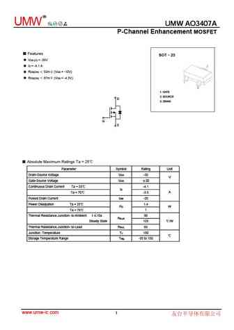
R UMW UMW AO3407A UMW AO3407A UMW AO3407A P-Channel Enhancement MOSFET Features SOT 23 VDS (V) = -30V ID = -4.1 A RDS(ON) 52m (VGS = -10V) RDS(ON) 87m (VGS = -4.5V) 1. GATE 2. SOURCE D 3. DRAIN G S Absolute Maximum Ratings Ta = 25 Parameter Symbol Rating Unit Drain-Source Voltage VDS -30 V Gate-Source Voltage VGS 20 Continuous Drain Current Ta = 25 -4.1
atm3407psa.pdf
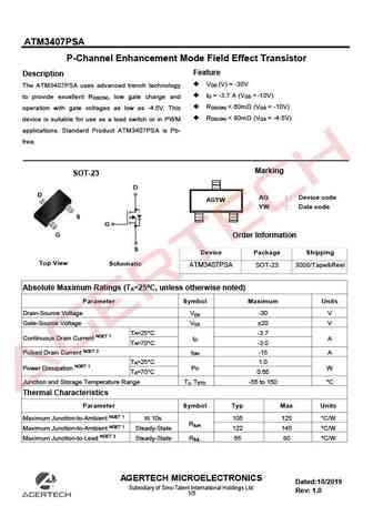
ATM3407PSA P-Channel Enhancement Mode Field Effect Transistor Feature Description V (V) = -30V DS The ATM3407PSA uses advanced trench technology I = -3.7 A (V =-10V) D GS to provide excellent R , low gate charge and DS(ON) R
as3407.pdf
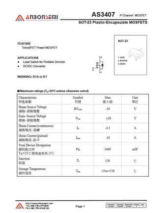
P-Channel MOSFET AS3407 SOT-23 Plastic-Encapsulate MOSFETS SOT-23 FEATURE TrenchFET Power MOSFET 1. GATE APPLICATIONS 2. SOURCE Load Switch for Portable Devices 3. DRAIN DC/DC Converter MARKING B 7 A or B 7 Maximum ratings (Ta=25 unless otherwise noted) Characteristic Symbol Max Unit Drain-Source Voltage BV -30 V DSS
bm3407a.pdf
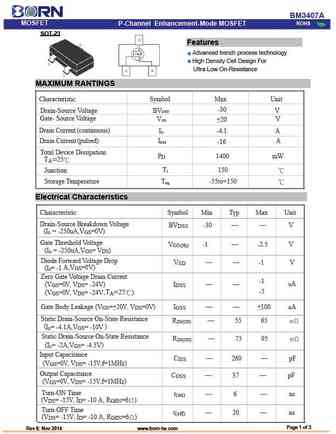
BM3407A MOSFET ROHS P-Channel Enhancement-Mode MOSFET SOT-23 - Features Advanced trench process technology High Density Cell Design For Ultra Low On-Resistance MAXIMUM RANTINGS Characteristic Symbol Max Unit -30 Drain-Source Voltage BV V DSS Gate- Source Voltage V V GS +20 Drain Current (continuous) I -4.1 A D Drain Current (pulsed) I A DM -16 Total Device Di
ev3407.pdf
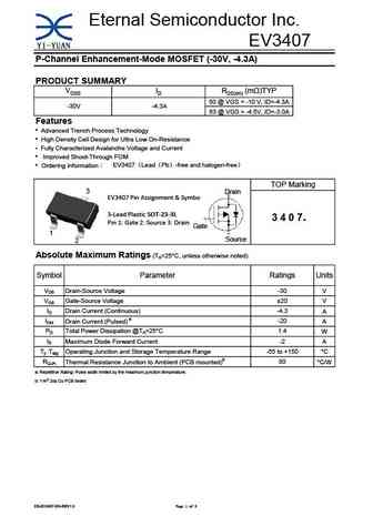
Eternal Semiconductor Inc. EV3407 P-Channel Enhancement-Mode MOSFET (-30V, -4.3A) PRODUCT SUMMARY VDSS ID RDS(on) (m )TYP 50 @ VGS = -10 V, ID=-4.3A -30V -4.3A 63 @ VGS = -4.5V, ID=-3.0A Features Advanced Trench Process Technology High Density Cell Design for Ultra Low On-Resistance Fully Characterized Avalanche Voltage and Current Improved Shoot-Through FOM O
ao3407.pdf
Plastic-Encapsulate Mosfets AO3407 FEATURES P-Channel MOSFET The AO3407 uses advanced trench technology to provide excellent RDS(ON) and low gate charge. This device is suitable for use as a load switch or in PWM applications. D D 1.Gate 2.Source SOT-23 G G 3.Drain S S Absolute Maximum Ratings (TA=25oC, unless otherwise noted) Parameter Symbol Value Unit Drain-Source Voltage
hss3407a.pdf
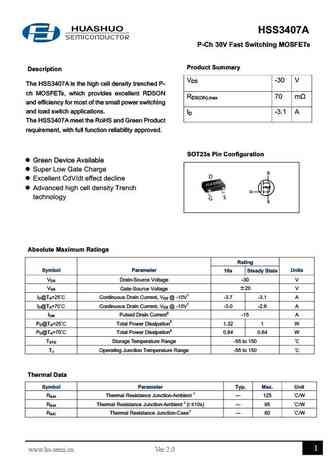
HSS3407A P-Ch 30V Fast Switching MOSFETs Product Summary Description VDS -30 V The HSS3407A is the high cell density trenched P- ch MOSFETs, which provides excellent RDSON RDS(ON),max 70 m and efficiency for most of the small power switching and load switch applications. ID -3.1 A The HSS3407A meet the RoHS and Green Product requirement, with full function reliability a
ao3407a.pdf
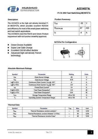
AO3407A P-Ch 30V Fast Switching MOSFETs Product Summary Description The AO3407A is the high cell density trenched P- V -30 V DS ch MOSFETs, which provides excellent RDSON R 47 m DS(ON),typ and efficiency for most of the small power switching and load switch applications. I -4 A D The AO3407A meet the RoHS and Green Product requirement with full function reliability a
jmtl3407a.pdf
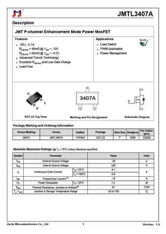
JMTL3407A Description JMT P-channel Enhancement Mode Power MosFET Features Applications -30V, -4.1A Load Switch RDS(ON)
jmtj3407a.pdf
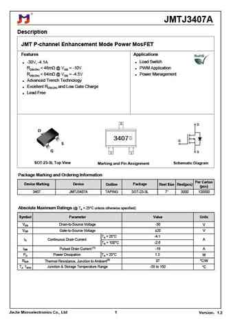
JMTJ3407A Description JMT P-channel Enhancement Mode Power MosFET Features Applications -30V, -4.1A Load Switch RDS(ON)
ao3407.pdf
AO3407 SOT-23 Plastic-Encapsulate MOSFETS SOT-23 30V P-Channel Advanced Power MOSFET 3 ID Max V(BR)DSS RDS(on)Typ 43m @ -10V 1. GATE - 4.1A -30V 2. SOURCE 66m @ -4.5V 1 3. DRAIN 2 FEATURE APPLICATION Low RDS(on) @VGS=-10V Load Switch -5V Logic Level Control Switching circuits High-speed line driver Power Management Functions M
pjm3407psa.pdf
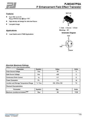
PJM3407PSA P Enhancement Field Effect Transistor SOT-23 Features VDS=-30V, ID=-4.1A RDS(on)=50m (Typ.)@VGS=-10V High density cell design for ultra low RDS(ON) Low gate charge 1. Gate 2.Source 3.Drain Marking R7 Applications Schematic Diagram Load Switch and in PWM Applications Drain 3 1 Gate Source 2 Absolute Maximum Ratings Ratings at TA =25 unless ot
ao3407.pdf
AO3407 -30V P-Channel Enhancement Mode MOSFET V = -30V DS R , V DS(ON) gs@-10V, I -4.1A
agm3407e.pdf
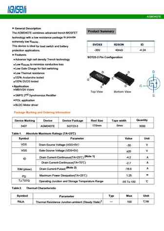
AGM3407E Table 3. Electrical Characteristics (TJ=25 unless otherwise noted) Symbol Parameter Conditions Min Typ Max Unit On/Off States BV Drain-Source Breakdown Voltage V =0V I =-250 A -30 -- -- V GS D DSS Zero Gate Voltage Drain Current V =-30V,V =0V -- -- -1 A DS GS I DSS V = 20V,V =0V -- -- nA GS DS IGSS Gate-Body Leakage Current 100 VGS(th) Gate Threshold Voltag
ao3407.pdf
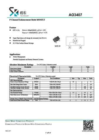
AO3407 P-Channel Enhancement Mode MOSFET Feature DS(ON) GS -30V/-4.1A, R =80m (MAX) @V = -10V. DS(ON) GS R = 100m (MAX) @V = -4.5V. . DS(ON) Super High dense cell design for extremely low R Reliable and Rugged SC-59 for Surface Mount Package SOT-59 Applications Power Management Portable Equipment and Battery Powered Systems. A T =25 Unless Ot
tdm3407.pdf
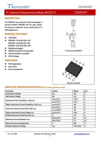
DATASHEET Techcode P-Channel Enhancement Mode MOSFET TDM3407 DESCRIPTION The TDM3407 uses advanced trench technology to provide excellent RDS(ON) and low gate charge. This device is suitable for use as a load switch or in PWM applications. GENERAL FEATURES 40V PMOS RDS(ON)
ao3407.pdf
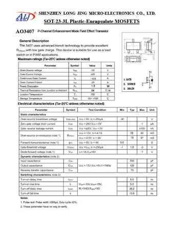
SHENZHEN LONG JING MICRO-ELECTRONICS CO., LTD. SOT-23-3L Plastic-Encapsulate MOSFETS Encapsu P-Channel Enhancement Mode Field Effect Transistor A O34 0 7 Maximum ratings (Ta=25 unless otherwise noted) 4.6 1.GATE 2. SOURCE 1.5 W 3. DRAIN 84 Electrical characteristics (Ta=25 unless otherwise noted) 55 75 1.5
tf3407.pdf
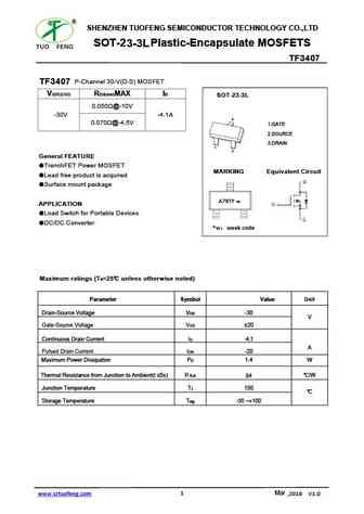
SHENZHEN TUOFENG SEMICONDUCTOR TECHNOLOGY CO.,LTD SOT-2 Plastic-Encapsulate MOSFETS 3-3L TF3407 P-Channel 30-V(D-S) MOSFET TF3407 V(BR)DSS RDS(on)MAX ID SOT-23-3L 0.050 @-10V -30V -4.1A 3 0.070 @-4.5V 1.GATE 2.SOURCE 3.DRAIN 1 2 General FEATURE TrenchFET Power MOSFET MARKING Equivalent Circuit Lead free product is acquired Surface mount package A79TF w APPLICAT
ao3407.pdf
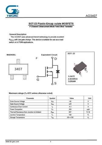
AO3407 SI2305 AO3401 SI2301 SOT-23 Plastic-Encap sulate MOSFETS P-Channel Enhancement Mode Field Effect Transistor P-Channel Enhancement Mode Field Effect Transistor P-Channel Enhancement Mode Field Effect Transistor P-Channel Enhancement Mode Field Effect Transistor P-Channel Enhancement Mode Field Effect Transistor SI2301 General Description The BC3407 uses advanced trench techno
wst3407a.pdf
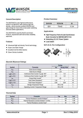
WST3407A P-Ch MOSFET Product Summery General Description The WST3407A is the highest performance BVDSS RDSON ID trench P-ch MOSFET with extreme high cell density , which provide excellent RDSON and -30V 75m -5.3A gate charge for most of the small power switching and load switch applications. Applications The WST3407A meet the RoHS and Green Product requirement with full
wst3407.pdf
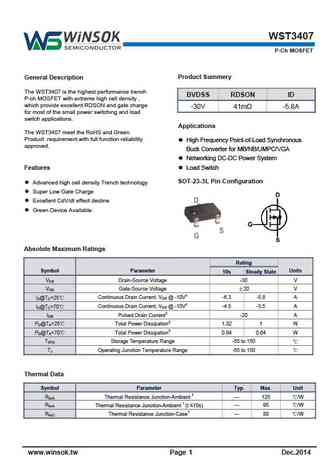
WST3407 P-Ch MOSFET Product Summery General Description The WST3407 is the highest performance trench BVDSS RDSON ID P-ch MOSFET with extreme high cell density , which provide excellent RDSON and gate charge -30V 41m -5.8A for most of the small power switching and load switch applications. Applications The WST3407 meet the RoHS and Green Product requirement with full fu
se3407.pdf
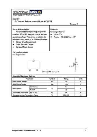
SE3407 P-Channel Enhancement-Mode MOSFET Revision A General Description Features For a single MOSFET Advanced trench technology to provide excellent RDS(ON), low gate charge and low V =-30V DS operation voltage. This device is suitable for R =40m @V =-10V DS(ON) GS using as a load switch or in PWM applications. Simple Drive Requirement Small Package Outline
sm3407.pdf
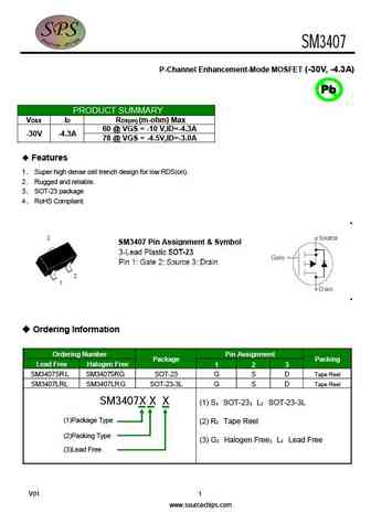
SM3407 P-Channel Enhancement-Mode MOSFET (-30V, -4.3A) Pb PRODUCT SUMMARY VDSS ID RDS(on) (m-ohm) Max 60 @ VGS = -10 V,ID=-4.3A -30V -4.3A 78 @ VGS = -4.5V,ID=-3.0A Features 1 Super high dense cell trench design for low RDS(on). 2 Rugged and reliable. 3 SOT-23 package 4 RoHS Compliant. SM3407 Pin Assignment & Symbol Ordering Information
ao3407.pdf
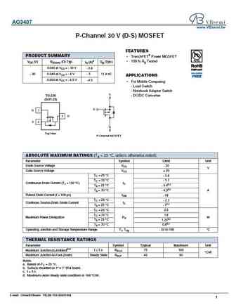
AO3407 www.VBsemi.tw P-Channel 30 V (D-S) MOSFET FEATURES PRODUCT SUMMARY TrenchFET Power MOSFET 100 % Rg Tested VDS (V) RDS(on) ( ) Typ. ID (A)a Qg (Typ.) 0.046 at VGS = - 10 V - 5.6 0.049 at VGS = - 6 V - 5 11.4 nC - 30 APPLICATIONS 0.054 at VGS = - 4.5 V -4.5 For Mobile Computing - Load Switch - Notebook Adaptor Switch S TO-236 - DC/DC Converter (SOT-23)
si3407dv-t1.pdf
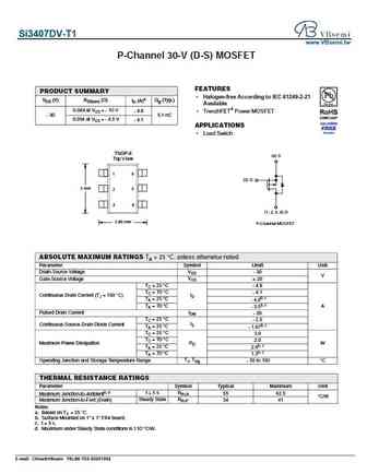
Si3407DV-T1 www.VBsemi.tw P-Channel 30-V (D-S) MOSFET FEATURES PRODUCT SUMMARY Halogen-free According to IEC 61249-2-21 VDS (V) RDS(on) ( ) ID (A)a Qg (Typ.) Available 0.049 at VGS = - 10 V - 4.8 TrenchFET Power MOSFET - 30 5.1 nC 0.054 at VGS = - 4.5 V - 4.1 APPLICATIONS Load Switch TSOP-6 (4) S Top V iew 1 6 (3) G 3 mm 5 2 3 4 (1, 2, 5, 6) D 2.85 mm P
smc3407s.pdf
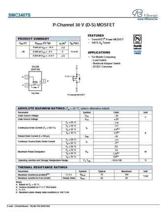
SMC3407S www.VBsemi.tw P-Channel 30 V (D-S) MOSFET FEATURES PRODUCT SUMMARY TrenchFET Power MOSFET 100 % Rg Tested VDS (V) RDS(on) ( ) Typ. ID (A)a Qg (Typ.) 0.046 at VGS = - 10 V - 5.6 0.049 at VGS = - 6 V - 5 11.4 nC - 30 APPLICATIONS 0.054 at VGS = - 4.5 V -4.5 For Mobile Computing - Load Switch - Notebook Adaptor Switch S TO-236 - DC/DC Converter (SOT-23
am3407pe.pdf
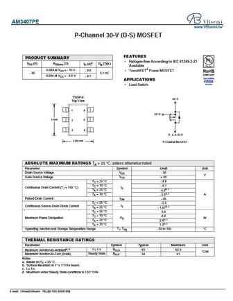
AM3407PE www.VBsemi.tw P-Channel 30-V (D-S) MOSFET FEATURES PRODUCT SUMMARY Halogen-free According to IEC 61249-2-21 VDS (V) RDS(on) ( ) ID (A)a Qg (Typ.) Available 0.049 at VGS = - 10 V - 4.8 TrenchFET Power MOSFET - 30 5.1 nC 0.054 at VGS = - 4.5 V - 4.1 APPLICATIONS Load Switch TSOP-6 (4) S Top V iew 1 6 (3) G 3 mm 5 2 3 4 (1, 2, 5, 6) D 2.85 mm P-Ch
yjl3407a.pdf
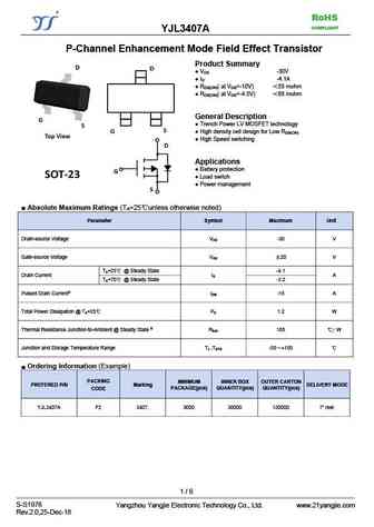
RoHS COMPLIANT YJL3407A P-Channel Enhancement Mode Field Effect Transistor Product Summary V -30V DS I -4.1A D R ( at V =-10V) 55 mohm DS(ON) GS R ( at V =-4.5V) 68 mohm DS(ON) GS General Description Trench Power LV MOSFET technology High density cell design for Low R DS(ON) High Speed switching Applications Battery protect
hm3407b.pdf
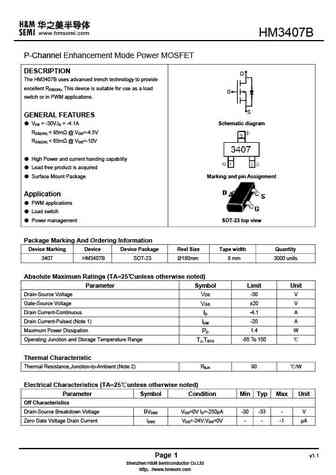
HM3407B P-Channel Enhancement Mode Power MOSFET DESCRIPTION D The HM3407B uses advanced trench technology to provide excellent RDS(ON), This device is suitable for use as a load G switch or in PWM applications. S GENERAL FEATURES VDS = -30V,ID = -4.1A Schematic diagram RDS(ON)
hm3407a.pdf
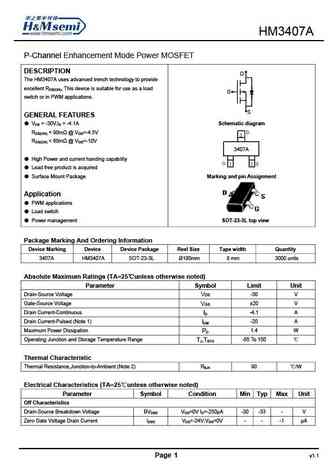
HM3407A P-Channel Enhancement Mode Power MOSFET DESCRIPTION D The HM3407A uses advanced trench technology to provide excellent RDS(ON), This device is suitable for use as a load G switch or in PWM applications. S GENERAL FEATURES VDS = -30V,ID = -4.1A Schematic diagram RDS(ON)
irfb3407z.pdf
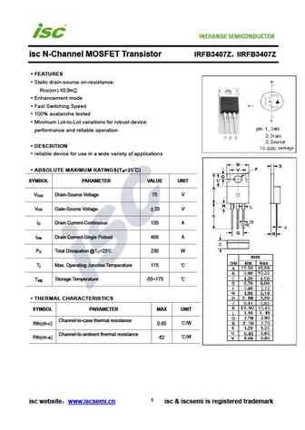
isc N-Channel MOSFET Transistor IRFB3407Z IIRFB3407Z FEATURES Static drain-source on-resistance RDS(on) 5.0m Enhancement mode Fast Switching Speed 100% avalanche tested Minimum Lot-to-Lot variations for robust device performance and reliable operation DESCRITION reliable device for use in a wide variety of applications ABSOLUTE MAXIMUM RATINGS(T =25 ) a
ap3407ai.pdf
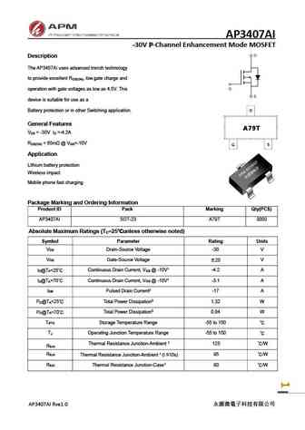
AP3407AI -30V P-Channel Enhancement Mode MOSFET Description The AP3407AI uses advanced trench technology to provide excellent R , low gate charge and DS(ON) operation with gate voltages as low as 4.5V. This device is suitable for use as a Battery protection or in other Switching application. General Features V = -30V I =-4.2A DS D R
ap3407mi.pdf
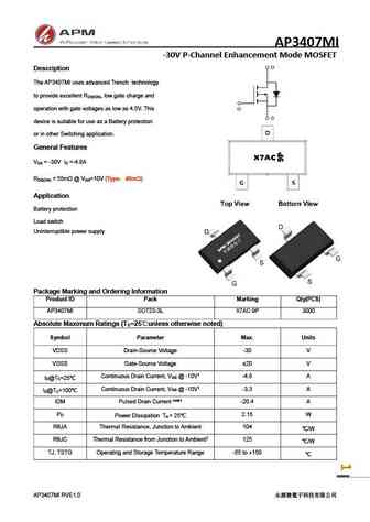
AP3407MI -30V P-Channel Enhancement Mode MOSFET Description The AP3407MI uses advanced Trench technology to provide excellent R , low gate charge and DS(ON) operation with gate voltages as low as 4.5V. This device is suitable for use as a Battery protection or in other Switching application. General Features V = -30V I =-4.8A DS D R
Otros transistores... TX50N06 , XG65T125PS1B , XG65T230PS1B , XGP6508B , XGP6510B , YWNM6001 , 2N7002AK , 2310 , AO3401 , SPA22N65G , SPA24N50G , SPA65R38G , SPA65R72G , SPC10N65G , SPC10N80G , SPC16N65G , SPC18N50G .
History: WMM020N06HG4 | 2SK1254S
History: WMM020N06HG4 | 2SK1254S
🌐 : EN ES РУ

Liste
Recientemente añadidas las descripciónes de los transistores:
MOSFET: AUB034N10 | AUB033N08BG | AUB026N085 | AUA062N08BG | AUA060N08AG | AUA056N08BGL | AUA039N10 | ASW80R290E | ASW65R120EFD | ASW65R110E | ASW65R095EFD | ASW65R046EFD | ASW65R041EFDA | ASW65R041E | ASW60R150E | ASW60R090EFDA
Popular searches
2sd669 datasheet | c102 transistor | bt152 datasheet | 2sa1302 datasheet | mpsa13 transistor equivalent | кт817г характеристики | 2sc1972 | 2n5088 transistor equivalent