7506 MOSFET Equivalente. Reemplazo. Hoja de especificaciones. Principales características
Número de Parte: 7506
Tipo de FET: MOSFET
Polaridad de transistor: N
ESPECIFICACIONES MÁXIMAS
Pdⓘ - Máxima
disipación de potencia: 29 W
|Vds|ⓘ - Voltaje máximo drenador-fuente: 30 V
|Vgs|ⓘ - Voltaje máximo fuente-puerta: 20 V
|Id|ⓘ - Corriente continua
de drenaje: 30 A
Tjⓘ - Temperatura máxima de unión: 150 °C
CARACTERÍSTICAS ELÉCTRICAS
trⓘ - Tiempo
de subida: 12 nS
Cossⓘ - Capacitancia de salida: 142 pF
RDSonⓘ - Resistencia estado encendido drenaje a fuente: 0.014 Ohm
Encapsulados: PDFN3X3-8
Búsqueda de reemplazo de 7506 MOSFET
- Selecciónⓘ de transistores por parámetros
7506 datasheet
..1. Size:3431K cn tuofeng
7506.pdf 
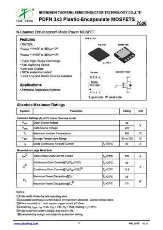
SHENZHEN TUOFENG SEMICONDUCTOR TECHNOLOGY CO.,LTD PDFN 3x3 Plastic-Encapsulate MOSFETS 7506 N-Channel Enhancement Mode Power MOSFET DFN 3x3_EP Features 30V/30A, Top View Bottom View RDS (ON) =10m (Typ.)@VGS=10V RDS (ON) =15m (Typ.)@VGS=4.5V Super High Dense Cell Design Pin 1 Fast Switching Speed Low gate Charge Equivalent Circuit Top View 100% avalanche t
0.1. Size:324K 1
aon7506.pdf
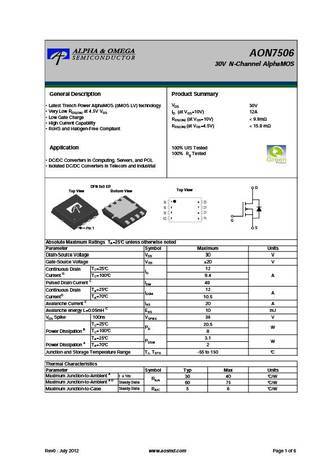
AON7506 30V N-Channel AlphaMOS General Description Product Summary VDS 30V Latest Trench Power AlphaMOS ( MOS LV) technology Very Low RDS(ON) at 4.5V VGS ID (at VGS=10V) 12A Low Gate Charge RDS(ON) (at VGS=10V)
0.2. Size:210K international rectifier
irf7506pbf.pdf
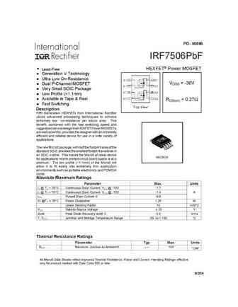
PD - 95696 IRF7506PbF Lead-Free www.irf.com 9/2/04 IRF7506PbF 2 www.irf.com IRF7506PbF www.irf.com 3 IRF7506PbF 4 www.irf.com IRF7506PbF www.irf.com 5 IRF7506PbF 6 www.irf.com IRF7506PbF Micro8 Package Outline LEAD ASSIGNMENTS INCHES MILLIMETERS DIM D MIN MAX MIN MAX 3 - B - D D D D D1 D1 D2 D2 A .036 .044 0.91 1.11 A1 .004 .008 0.10 0.20 8 7 6 5 8 7 6 5 B
0.3. Size:103K international rectifier
irf7506.pdf
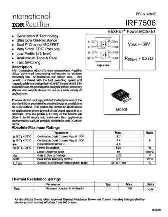
PD - 9.1268F IRF7506 HEXFET Power MOSFET Generation V Technology 1 8 Ultra Low On-Resistance S1 D1 VDSS = -30V Dual P-Channel MOSFET 2 7 G1 D1 Very Small SOIC Package 3 6 S2 D2 Low Profile (
0.4. Size:320K philips
buk7506-55a buk7606-55a.pdf
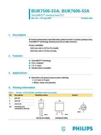
BUK7506-55A; BUK7606-55A TrenchMOS standard level FET Rev. 02 03 July 2001 Product data 1. Description N-channel enhancement mode field-effect power transistor in a plastic package using TrenchMOS technology, featuring very low on-state resistance. Product availability BUK7506-55A in SOT78 (TO-220AB) BUK7606-55A in SOT404 (D2-PAK). 2. Features TrenchMOS technology Q10
0.5. Size:51K philips
buk7506-55a 1.pdf
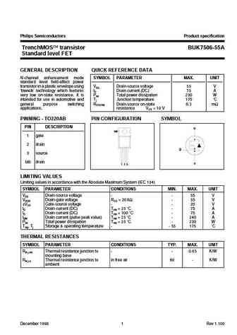
Philips Semiconductors Product specification TrenchMOS transistor BUK7506-55A Standard level FET GENERAL DESCRIPTION QUICK REFERENCE DATA N-channel enhancement mode SYMBOL PARAMETER MAX. UNIT standard level field-effect power transistor in a plastic envelope using VDS Drain-source voltage 55 V trench technology which features ID Drain current (DC) 75 A very low on-state resis
0.6. Size:322K philips
buk7506-75b buk7606-75b.pdf
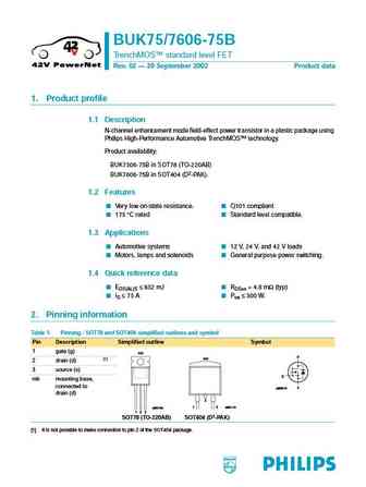
BUK75/7606-75B TrenchMOS standard level FET Rev. 02 20 September 2002 Product data 1. Product profile 1.1 Description N-channel enhancement mode field-effect power transistor in a plastic package using Philips High-Performance Automotive TrenchMOS technology. Product availability BUK7506-75B in SOT78 (TO-220AB) BUK7606-75B in SOT404 (D2-PAK). 1.2 Features Very low on-stat
0.7. Size:49K philips
buk7506-30 1.pdf
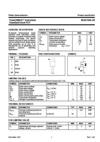
Philips Semiconductors Product specification TrenchMOS transistor BUK7506-30 Standard level FET GENERAL DESCRIPTION QUICK REFERENCE DATA N-channel enhancement mode SYMBOL PARAMETER MAX. UNIT standard level field-effect power transistor in a plastic envelope using VDS Drain-source voltage 30 V trench technology. The device ID Drain current (DC) 75 A features very low on-state
0.8. Size:406K panasonic
dsa7506.pdf
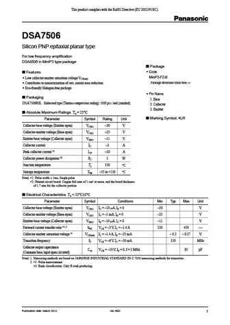
This product complies with the RoHS Directive (EU 2002/95/EC). DSA7506 Silicon PNP epitaxial planar type For low frequency amplification DSA8506 in MiniP3 type package Package Code Features MiniP3-F2-B Low collector-emitter saturation voltage VCE(sat) Package dimension clicks here. Click! Contributes to miniaturization of sets, mount area reduction Eco-fr
0.9. Size:528K texas
csd17506q5a.pdf
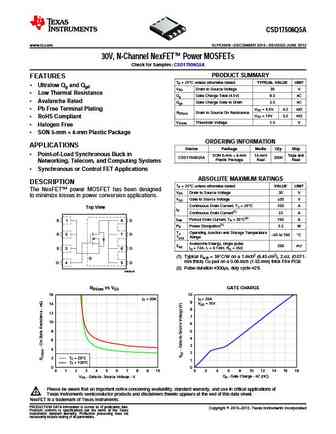
CSD17506Q5A www.ti.com SLPS304B DECEMBER 2010 REVISED JUNE 2012 30V, N-Channel NexFET Power MOSFETs Check for Samples CSD17506Q5A PRODUCT SUMMARY 1 FEATURES TA = 25 C unless otherwise stated TYPICAL VALUE UNIT 2 Ultralow Qg and Qgd VDS Drain to Source Voltage 30 V Low Thermal Resistance Qg Gate Charge Total (4.5V) 8.3 nC Avalanche Rated Qgd Gate Charge Gat
0.10. Size:324K aosemi
aon7506.pdf

AON7506 30V N-Channel AlphaMOS General Description Product Summary VDS 30V Latest Trench Power AlphaMOS ( MOS LV) technology Very Low RDS(ON) at 4.5V VGS ID (at VGS=10V) 12A Low Gate Charge RDS(ON) (at VGS=10V)
0.11. Size:185K sino
sm7506nfp.pdf
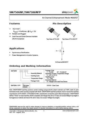
SM7506NF/SM7506NFP N-Channel Enhancement Mode MOSFET Features Pin Description 75V/170A**, RDS(ON)= 4.3m (max.) @ VGS= 10V Reliable and Rugged S S D D Lead Free and Green Devices Available G G (RoHS Compliant) Top View of TO-220-FP Top View of TO-220 D Applications G Synchronous Rectification. Power Management in Inverter Systems. S N-Channel MOSFET Order
0.12. Size:283K sino
sm7506nsw.pdf
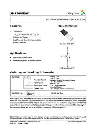
SM7506NSW N-Channel Enhancement Mode MOSFET Features Pin Description 75V/170A**, RDS(ON)= 4.3m (max.) @ VGS= 10V Reliable and Rugged S D Lead Free and Green Devices Available G (RoHS Compliant) Top View of TO-247 D Applications G Synchronous Rectification. Power Management in Inverter Systems. S N-Channel MOSFET Ordering and Marking Information Package Code SM7506
0.13. Size:280K sino
sm7506nf.pdf
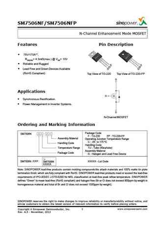
SM7506NF/SM7506NFP N-Channel Enhancement Mode MOSFET Features Pin Description 75V/170A**, RDS(ON)= 4.3m (max.) @ VGS= 10V Reliable and Rugged S S D D Lead Free and Green Devices Available G G (RoHS Compliant) Top View of TO-220-FP Top View of TO-220 D Applications G Synchronous Rectification. Power Management in Inverter Systems. S N-Channel MOSFET Ordering and Mar
0.14. Size:80K kexin
krf7506.pdf
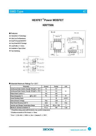
SMD Type IC SMD Type IC HEXFET Power MOSFET KRF7506 Features Generation V Technology Ultra Low On-Resistance Dual P-Channel MOSFET Very Small SOIC Package Low Profile ( 1.1mm) Available in Tape & Reel Fast Switching Absolute Maximum Ratings Ta = 25 Parameter Symbol Rating Unit Continuous Drain Current, VGS @-10V@TA =25 ID -1.7 Continuous Drain Current, VGS @-10V@TA =70 ID -1.4 A
0.15. Size:281K inchange semiconductor
buk7506-55a.pdf
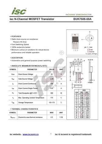
isc N-Channel MOSFET Transistor BUK7506-55A FEATURES Static drain-source on-resistance RDS(on) 6.3m Fast Switching Speed 100% avalanche tested Minimum Lot-to-Lot variations for robust device performance and reliable operation DESCRITION Automotive and general purpose power switching ABSOLUTE MAXIMUM RATINGS(T =25 ) a SYMBOL PARAMETER VALUE UNIT V Drain-Sour
Otros transistores... 4803A
, 6435
, 6764
, 7240
, 7409
, 7409B
, 7410
, 7430
, STP65NF06
, 7788
, 8810B
, 90N03L
, S8205B
, SIA517
, SLP6N70U
, SLF6N70U
, TF2015
.
