2SK3653 MOSFET Equivalente. Reemplazo. Hoja de especificaciones. Principales características
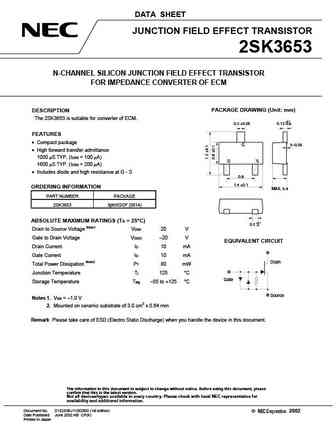
Número de Parte: 2SK3653
Tipo de FET: JFET
Polaridad de transistor: N
ESPECIFICACIONES MÁXIMAS
Pdⓘ - Máxima
disipación de potencia: 0.08 W
|Vds|ⓘ - Voltaje máximo drenador-fuente: 20 V
|Id|ⓘ - Corriente continua
de drenaje: 0.01 A
Tjⓘ - Temperatura máxima de unión: 125 °C
CARACTERÍSTICAS ELÉCTRICAS
RDSonⓘ - Resistencia estado encendido drenaje a fuente: 1000 Ohm
Encapsulados: XSOF
Búsqueda de reemplazo de 2SK3653 MOSFET
- Selecciónⓘ de transistores por parámetros
2SK3653 datasheet
..1. Size:43K nec
2sk3653.pdf 

DATA SHEET JUNCTION FIELD EFFECT TRANSISTOR 2SK3653 N-CHANNEL SILICON JUNCTION FIELD EFFECT TRANSISTOR FOR IMPEDANCE CONVERTER OF ECM PACKAGE DRAWING (Unit mm) DESCRIPTION The 2SK3653 is suitable for converter of ECM. +0.1 0.3 0.05 0.13 0.05 FEATURES Compact package G 0 0.05 High forward transfer admittance 1000 S TYP. (IDSS = 100 A) D S 1600 S TYP. (IDSS =
8.1. Size:391K toshiba
2sk3658.pdf 

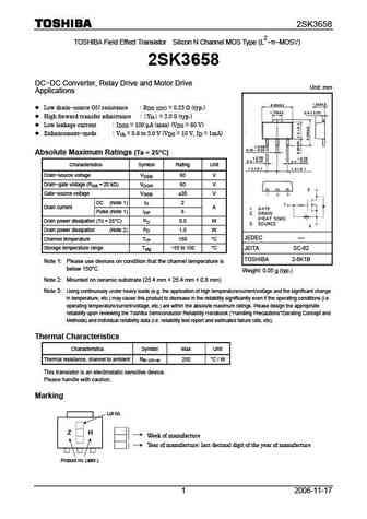
2SK3658 2 TOSHIBA Field Effect Transistor Silicon N Channel MOS Type (L - -MOSV) 2SK3658 DC-DC Converter, Relay Drive and Motor Drive Unit mm Applications Low drain-source ON resistance RDS (ON) = 0.23 (typ.) High forward transfer admittance Yfs = 2.0 S (typ.) Low leakage current IDSS = 100 A (max) (VDS = 60 V) Enhancement-mode Vth = 0.8 to 2.0 V (VD
8.2. Size:679K toshiba
2sk365.pdf 

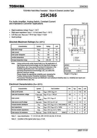
2SK365 TOSHIBA Field Effect Transistor Silicon N Channel Junction Type 2SK365 For Audio Amplifier, Analog-Switch, Constant Current Unit mm and Impedance Converter Applications High breakdown voltage VGDS = -50 V High input impedance IGSS = -1.0 nA (max) (VGS = -30 V) Low RDS (ON) RDS (ON) = 80 (typ.) (IDSS = 5 mA) Small package Absolute Maximum Rating
8.3. Size:157K toshiba
2sk3656.pdf 

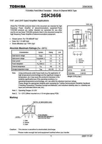
2SK3656 TOSHIBA Field Effect Transistor Silicon N Channel MOS Type 2SK3656 VHF- and UHF-band Amplifier Applications Unit mm (Note)The TOSHIBA products listed in this document are intended for high frequency Power Amplifier of telecommunications equipment.These TOSHIBA products are neither intended nor warranted for any other use.Do not use these TOSHIBA products listed in this
8.4. Size:204K renesas
2sk3659.pdf 

To our customers, Old Company Name in Catalogs and Other Documents On April 1st, 2010, NEC Electronics Corporation merged with Renesas Technology Corporation, and Renesas Electronics Corporation took over all the business of both companies. Therefore, although the old company name remains in this document, it is a valid Renesas Electronics document. We appreciate your understanding.
8.5. Size:114K fuji
2sk3651-01r.pdf 

2SK3651-01R [0311] FUJI POWER MOSFET N-CHANNEL SILICON POWER MOSFET Super FAP-G Series Outline Drawings (mm) Features TO-3PF High speed switching Low on-resistance No secondary breadown Low driving power Avalanche-proof Applications Switching regulators UPS (Uninterruptible Power Supply) DC-DC converters Maximum ratings and characteristicAbsolute maximum ratings (Tc=25 C unle
8.6. Size:254K fuji
2sk3650-01l-s-sj.pdf 

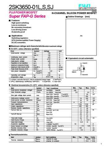
2SK3650-01L,S,SJ 200304 FUJI POWER MOSFET N-CHANNEL SILICON POWER MOSFET Outline Drawings [mm] Super FAP-G Series Features High speed switching Low on-resistance No secondary breadown Low driving power Avalanche-proof Applications P4 Switching regulators UPS (Uninterruptible Power Supply) DC-DC converters Maximum ratings and characteristicAbsolute maximum ratings (Tc=25 C unl
8.7. Size:42K kexin
2sk3652.pdf 

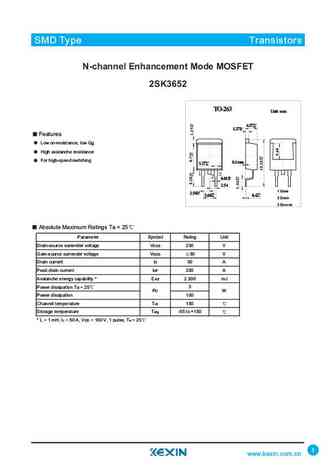
SMD Type IC SMD Type Transistors N-channel Enhancement Mode MOSFET 2SK3652 TO-263 Unit mm +0.2 4.57-0.2 1.27+0.1 -0.1 Features Low on-resistance, low Qg High avalanche resistance For high-speed switching 0.1max 1.27+0.1 -0.1 +0.1 0.81-0.1 2.54 1Gate 2.54+0.2 +0.2 -0.2 +0.1 5.08-0.1 0.4-0.2 2Drain 3 Source Absolute Maximum Ratings Ta = 25 Parameter Symbol Rating Unit
8.8. Size:356K inchange semiconductor
2sk3650-01sj.pdf 
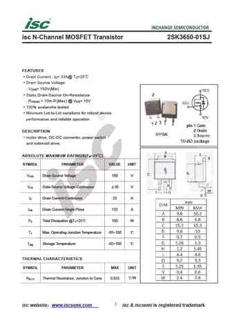
isc N-Channel MOSFET Transistor 2SK3650-01SJ FEATURES Drain Current I = 33A@ T =25 D C Drain Source Voltage V = 150V(Min) DSS Static Drain-Source On-Resistance R = 70m (Max) @ V = 10V DS(on) GS 100% avalanche tested Minimum Lot-to-Lot variations for robust device performance and reliable operation DESCRIPTION motor drive, DC-DC converter, power switch and so
8.9. Size:278K inchange semiconductor
2sk3659.pdf 
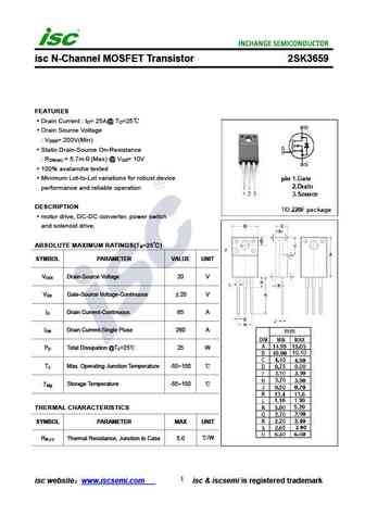
isc N-Channel MOSFET Transistor 2SK3659 FEATURES Drain Current I = 25A@ T =25 D C Drain Source Voltage V = 200V(Min) DSS Static Drain-Source On-Resistance R = 5.7m (Max) @ V = 10V DS(on) GS 100% avalanche tested Minimum Lot-to-Lot variations for robust device performance and reliable operation DESCRIPTION motor drive, DC-DC converter, power switch and soleno
8.10. Size:274K inchange semiconductor
2sk3651-01r.pdf 
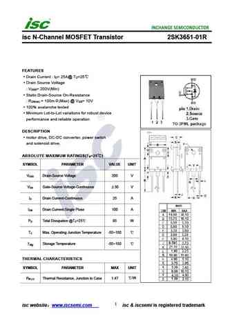
isc N-Channel MOSFET Transistor 2SK3651-01R FEATURES Drain Current I = 25A@ T =25 D C Drain Source Voltage V = 200V(Min) DSS Static Drain-Source On-Resistance R = 100m (Max) @ V = 10V DS(on) GS 100% avalanche tested Minimum Lot-to-Lot variations for robust device performance and reliable operation DESCRIPTION motor drive, DC-DC converter, power switch and so
8.11. Size:356K inchange semiconductor
2sk3650-01s.pdf 

isc N-Channel MOSFET Transistor 2SK3650-01S FEATURES Drain Current I = 33A@ T =25 D C Drain Source Voltage V = 150V(Min) DSS Static Drain-Source On-Resistance R = 70m (Max) @ V = 10V DS(on) GS 100% avalanche tested Minimum Lot-to-Lot variations for robust device performance and reliable operation DESCRIPTION motor drive, DC-DC converter, power switch and sol
8.12. Size:283K inchange semiconductor
2sk3650-01l.pdf 
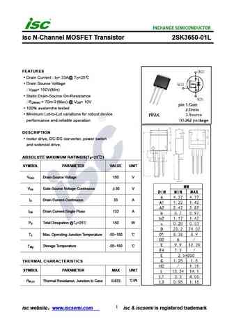
isc N-Channel MOSFET Transistor 2SK3650-01L FEATURES Drain Current I = 33A@ T =25 D C Drain Source Voltage V = 150V(Min) DSS Static Drain-Source On-Resistance R = 70m (Max) @ V = 10V DS(on) GS 100% avalanche tested Minimum Lot-to-Lot variations for robust device performance and reliable operation DESCRIPTION motor drive, DC-DC converter, power switch and sol
Otros transistores... BUZ81
, FCA47N60F109
, FQP10N60C
, FQPF10N60C
, FCA47N60F
, FCA76N60N
, 2SJ245
, FCB11N60
, IRLZ44N
, FCB20N60
, 2SK3057
, 2SK3469-01MR
, FCB20N60F
, FCB36N60N
, 2SJ279
, FCD4N60
, IRFD9020
.
