DMN6040SK3-13 MOSFET Equivalente. Reemplazo. Hoja de especificaciones. Principales características
Número de Parte: DMN6040SK3-13
Tipo de FET: MOSFET
Polaridad de transistor: N
ESPECIFICACIONES MÁXIMAS
Pdⓘ - Máxima disipación de potencia: 100 W
|Vds|ⓘ - Voltaje máximo drenador-fuente: 60 V
|Vgs|ⓘ - Voltaje máximo fuente-puerta: 20 V
|Id|ⓘ - Corriente continua de drenaje: 35 A
Tjⓘ - Temperatura máxima de unión: 175 °C
CARACTERÍSTICAS ELÉCTRICAS
trⓘ - Tiempo de subida: 15 nS
Cossⓘ - Capacitancia de salida: 140 pF
RDSonⓘ - Resistencia estado encendido drenaje a fuente: 0.031 Ohm
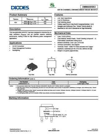
Encapsulados: TO252
Búsqueda de reemplazo de DMN6040SK3-13 MOSFET
- Selecciónⓘ de transistores por parámetros
DMN6040SK3-13 datasheet
dmn6040sk3-13.pdf
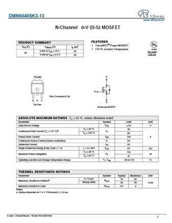
DMN6040SK3-13 www.VBsemi.tw N-Channel 6 0-V (D-S) MOSFET FEATURES PRODUCT SUMMARY TrenchFET Power MOSFET VDS (V) rDS(on) ( ) ID (A)a Available 175 C Junction Temperature 0.025 at VGS = 10 V 35 RoHS* 60 0.030 at VGS = 4.5 V 30 COMPLIANT TO-252 D G Drain Connected to Tab G D S S Top View N-Channel MOSFET ABSOLUTE MAXIMUM RATINGS TC = 25 C, unless otherwi
dmn6040sk3.pdf
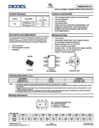
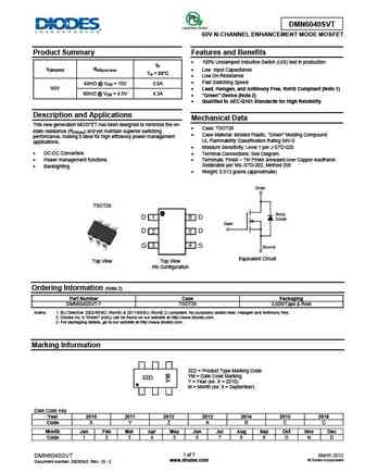
DMN6040SK3 60V N-CHANNEL ENHANCEMENT MODE MOSFET Product Summary Features ID Low Input Capacitance V(BR)DSS RDS(on) max TC = +25 C Low On-Resistance 40m @ VGS = 10V 20A Fast Switching Speed 60V 50m @ VGS = 4.5V 16A Totally Lead-Free & Fully RoHS Compliant (Notes 1 & 2) Halogen and Antimony Free. Green Device (Note 3) Qualified to AEC-Q1
dmn6040sk3.pdf
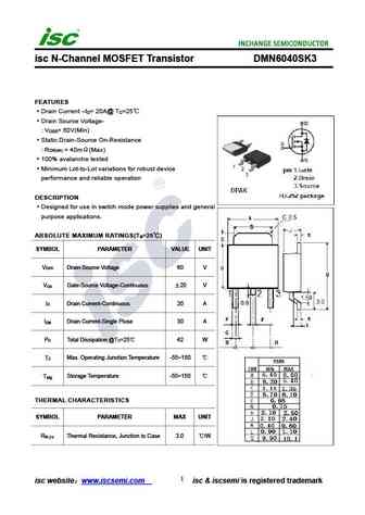
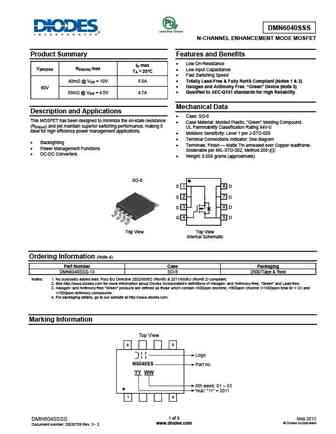
isc N-Channel MOSFET Transistor DMN6040SK3 FEATURES Drain Current I = 20A@ T =25 D C Drain Source Voltage- V = 60V(Min) DSS Static Drain-Source On-Resistance R = 40m (Max) DS(on) 100% avalanche tested Minimum Lot-to-Lot variations for robust device performance and reliable operation DESCRIPTION Designed for use in switch mode power supplies and general purp
dmn6040ssd.pdf
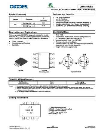
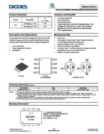
DMN6040SSD 60V DUAL N-CHANNEL ENHANCEMENT MODE MOSFET Product Summary Features and Benefits Low Input Capacitance ID Low On-Resistance V(BR)DSS RDS(on) max TA = +25 C Fast Switching Speed Totally Lead-Free & Fully RoHS Compliant (Notes 1 & 2) 40m @ VGS = 10V 5.0A Halogen and Antimony Free. Green Device (Note 3) 60V 4.4A Qualified to AEC
Otros transistores... DMC2038LVT-7-F , DMC2700UDM-7 , DMC3018LSD-13 , DMG1013UW-7 , DMG3420U-7 , DMG6602S , DMG6968U-7 , DMN4468LSS-13 , IRFP250 , DMN6068LK3-13 , DMN6068SE-13 , DMP3025LK3-13 , DMP3056LSD-13 , DTM4926 , DTM4946 , DTU09N03 , E10P02 .
History: SNN0310Q | IRFP7530
🌐 : EN ES РУ

Liste
Recientemente añadidas las descripciónes de los transistores:
MOSFET: AUB034N10 | AUB033N08BG | AUB026N085 | AUA062N08BG | AUA060N08AG | AUA056N08BGL | AUA039N10 | ASW80R290E | ASW65R120EFD | ASW65R110E | ASW65R095EFD | ASW65R046EFD | ASW65R041EFDA | ASW65R041E | ASW60R150E | ASW60R090EFDA
Popular searches
lm317t datasheet | irf540 | bc337 | ksc1845 | c1815 transistor | 2sc1815 | irfz44 | 2n5551