SI2302DS-T1-GE3 MOSFET Equivalente. Reemplazo. Hoja de especificaciones. Principales características
Número de Parte: SI2302DS-T1-GE3
Tipo de FET: MOSFET
Polaridad de transistor: N
ESPECIFICACIONES MÁXIMAS
Pdⓘ - Máxima disipación de potencia: 1.25 W
|Vds|ⓘ - Voltaje máximo drenador-fuente: 20 V
|Vgs|ⓘ - Voltaje máximo fuente-puerta: 12 V
|Id|ⓘ - Corriente continua de drenaje: 5 A
Tjⓘ - Temperatura máxima de unión: 150 °C
CARACTERÍSTICAS ELÉCTRICAS
trⓘ - Tiempo de subida: 17 nS
Cossⓘ - Capacitancia de salida: 105 pF
RDSonⓘ - Resistencia estado encendido drenaje a fuente: 0.028 typ Ohm
Encapsulados: SOT23
Búsqueda de reemplazo de SI2302DS-T1-GE3 MOSFET
- Selecciónⓘ de transistores por parámetros
SI2302DS-T1-GE3 datasheet
si2302ds-t1-ge3.pdf
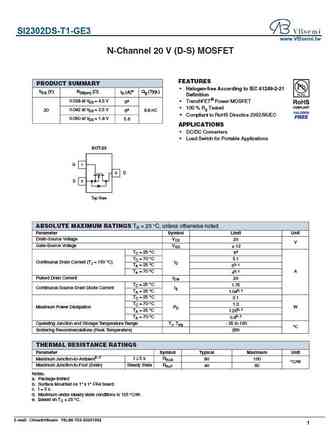
SI2302DS-T1-GE3 www.VBsemi.tw N-Channel 20 V (D-S) MOSFET FEATURES PRODUCT SUMMARY Halogen-free According to IEC 61249-2-21 VDS (V) RDS(on) ( ) ID (A)e Qg (Typ.) Definition 0.028 at VGS = 4.5 V TrenchFET Power MOSFET 6a 100 % Rg Tested 20 0.042 at VGS = 2.5 V 6a 8.8 nC Compliant to RoHS Directive 2002/95/EC 0.050 at VGS = 1.8 V 5.6 APPLICATIONS DC/D
si2302ds-3.pdf
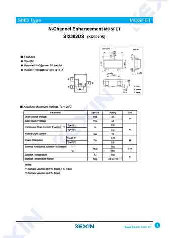
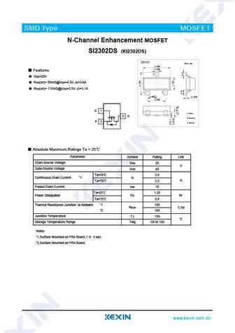
SMD Type MOSFET N-Channel Enhancement MOSFET SI2302DS (KI2302DS) SOT-23-3 Unit mm +0.2 2.9 -0.1 +0.1 0.4-0.1 3 Features VDS=20V RDS(on)= 85m @VGS=4.5V ,ID=3.6A RDS(on)= 115m @VGS=2.5V ,ID=3.1A 1 2 +0.02 +0.1 0.15 -0.02 0.95 -0.1 +0.1 1.9 -0.2 G 1 3 D 1. Gate S 2 2. Source 3. Drain Absolute Maximum Ratings Ta = 25 Parameter Symbol Rating Un
si2302ds.pdf
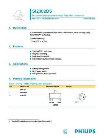
SI2302DS N-channel enhancement mode field-effect transistor Rev. 02 20 November 2001 Product data M3D088 1. Description N-channel enhancement mode field-effect transistor in a plastic package using TrenchMOS 1 technology. Product availability SI2302DS in SOT23. 2. Features TrenchMOS technology Very fast switching Logic level compatible Subminiature surface mount packa
si2302ds.pdf
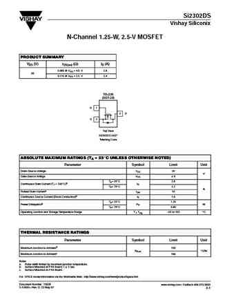
Si2302DS Vishay Siliconix N-Channel 1.25-W, 2.5-V MOSFET PRODUCT SUMMARY VDS (V) rDS(on) (W) ID (A) 0.085 @ VGS = 4.5 V 2.8 20 20 0.115 @ VGS = 2.5 V 2.4 TO-236 (SOT-23) G 1 3 D S 2 Top View Si2302DS (A2)* *Marking Code ABSOLUTE MAXIMUM RATINGS (TA = 25_C UNLESS OTHERWISE NOTED) Parameter Symbol Limit Unit Drain-Source Voltage VDS 20 V V Gate-Source Voltage VGS "8 TA= 25_
Otros transistores... SI1967DH-T1-GE3 , SI2300BDS-T1-GE3 , SI2300DS-T1-GE3 , SI2301ADS-T1 , SI2301BDS-T1-GE3 , SI2301CDS-T1 , SI2301DS-T1-GE3 , SI2302CDS-T1-GE3 , IRF3710 , SI2305ADS-T1-GE3 , SI2305CDS-T1-GE3 , SI2305DS-T1-GE3 , SI2309CDS-T1-GE3 , SI2312BDS-T1 , SI2312CDS-T1-GE3 , SI2324DS-T1-GE3 , SI2333CDS-T1-GE3 .
History: CS10N60FA9R
History: CS10N60FA9R
🌐 : EN ES РУ

Liste
Recientemente añadidas las descripciónes de los transistores:
MOSFET: AUB034N10 | AUB033N08BG | AUB026N085 | AUA062N08BG | AUA060N08AG | AUA056N08BGL | AUA039N10 | ASW80R290E | ASW65R120EFD | ASW65R110E | ASW65R095EFD | ASW65R046EFD | ASW65R041EFDA | ASW65R041E | ASW60R150E | ASW60R090EFDA
Popular searches
2sd555 | a950 transistor | k2611 | c1740 transistor | c828 transistor | c4467 | c2383 transistor | 2n3055 equivalent