NCE01P03S Datasheet. Equivalente. Reemplazo. Hoja de especificaciones. Principales características
Número de Parte: NCE01P03S 📄📄
Tipo de FET: MOSFET
Polaridad de transistor: P
ESPECIFICACIONES MÁXIMAS
Pdⓘ - Máxima disipación de potencia: 2.5 W
|Vds|ⓘ - Voltaje máximo drenador-fuente: 100 V
|Vgs|ⓘ - Voltaje máximo fuente-puerta: 20 V
|Id|ⓘ - Corriente continua de drenaje: 3 A
Tjⓘ - Temperatura máxima de unión: 150 °C
CARACTERÍSTICAS ELÉCTRICAS
trⓘ - Tiempo de subida: 18 nS
Cossⓘ - Capacitancia de salida: 260 pF
RDSonⓘ - Resistencia estado encendido drenaje a fuente: 0.2 Ohm
Encapsulados: SOP8
📄📄 Copiar
Búsqueda de reemplazo de NCE01P03S MOSFET
- Selecciónⓘ de transistores por parámetros
NCE01P03S datasheet
..1. Size:350K ncepower
nce01p03s.pdf 
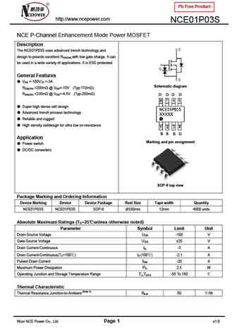
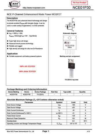
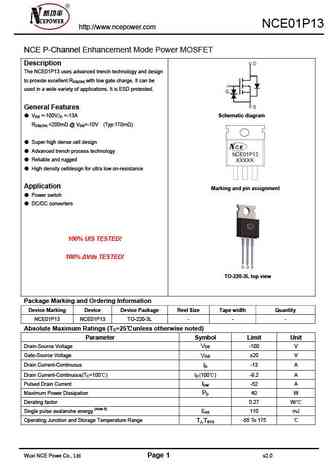
Pb Free Product http //www.ncepower.com NCE01P03S NCE P-Channel Enhancement Mode Power MOSFET Description The NCE01P03S uses advanced trench technology and design to provide excellent RDS(ON) with low gate charge. It can be used in a wide variety of applications. It is ESD protested. General Features VDS =-100V,ID =-3A Schematic diagram RDS(ON)
7.1. Size:384K ncepower
nce01p05s.pdf
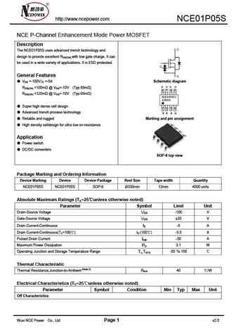
http //www.ncepower.com NCE01P05S NCE P-Channel Enhancement Mode Power MOSFET Description The NCE01P05S uses advanced trench technology and design to provide excellent RDS(ON) with low gate charge. It can be used in a wide variety of applications. It is ESD protested. General Features VDS =-100V,ID =-5A Schematic diagram RDS(ON)
8.1. Size:670K ncepower
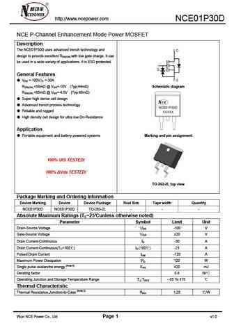
nce01p30k.pdf
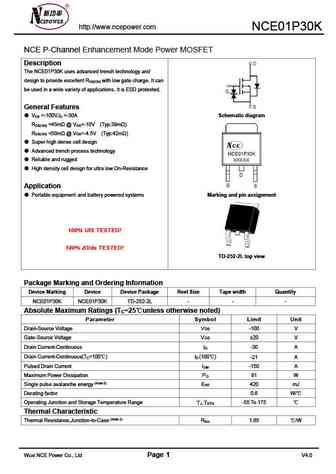
http //www.ncepower.com NCE01P30K NCE P-Channel Enhancement Mode Power MOSFET Description The NCE01P30K uses advanced trench technology and design to provide excellent R with low gate charge. It can DS(ON) be used in a wide variety of applications. It is ESD protested. General Features V =-100V,I =-30A Schematic diagram DS D R
8.2. Size:343K ncepower
nce01p18l.pdf
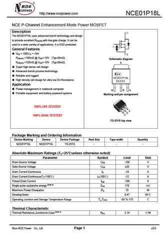
http //www.ncepower.com NCE01P18L NCE P-Channel Enhancement Mode Power MOSFET Description The NCE01P18L uses advanced trench technology and design to provide excellent RDS(ON) with low gate charge. It can be used in a wide variety of applications. It is ESD protested. General Features VDS =-100V,ID =-18A RDS(ON)
8.3. Size:562K ncepower
nce01p18d.pdf
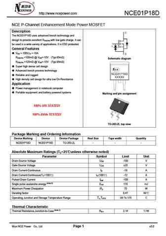
http //www.ncepower.com NCE01P18D NCE P-Channel Enhancement Mode Power MOSFET Description The NCE01P18D uses advanced trench technology and design to provide excellent RDS(ON) with low gate charge. It can be used in a wide variety of applications. It is ESD protested. General Features VDS =-100V,ID =-18A RDS(ON)
8.4. Size:713K ncepower
nce01p18.pdf
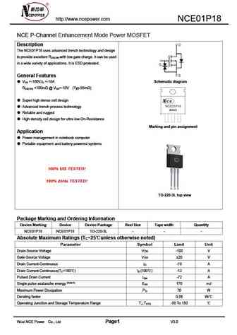
http //www.ncepower.com NCE01P18 NCE P-Channel Enhancement Mode Power MOSFET Description The NCE01P18 uses advanced trench technology and design to provide excellent R with low gate charge. It can be used DS(ON) in a wide variety of applications. It is ESD protested. General Features V =-100V,I =-18A Schematic diagram DS D R
8.5. Size:739K ncepower
nce01p13i.pdf
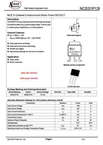
http //www.ncepower.com NCE01P13I NCE P-Channel Enhancement Mode Power MOSFET Description The NCE01P13I uses advanced trench technology and design to provide excellent R with low gate charge. It can be used DS(ON) in a wide variety of applications. It is ESD protested. General Features V =-100V,I =-13A Schematic diagram DS D R
8.6. Size:316K ncepower
nce01p30i.pdf
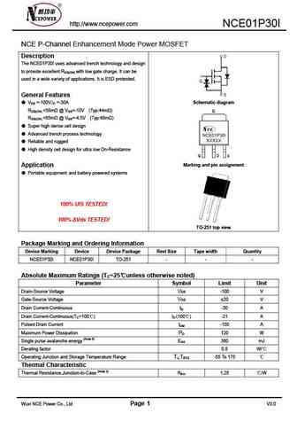
http //www.ncepower.com NCE01P30I NCE P-Channel Enhancement Mode Power MOSFET Description The NCE01P30I uses advanced trench technology and design to provide excellent RDS(ON) with low gate charge. It can be used in a wide variety of applications. It is ESD protested. General Features VDS =-100V,ID =-30A Schematic diagram RDS(ON)
8.7. Size:430K ncepower
nce01p18k.pdf
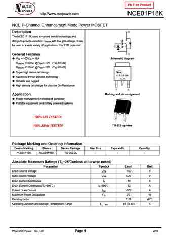
Pb Free Product http //www.ncepower.com NCE01P18K NCE P-Channel Enhancement Mode Power MOSFET Description The NCE01P18K uses advanced trench technology and design to provide excellent RDS(ON) with low gate charge. It can be used in a wide variety of applications. It is ESD protested. General Features VDS =-100V,ID =-18A Schematic diagram RDS(ON)
8.9. Size:297K ncepower
nce01p30l.pdf
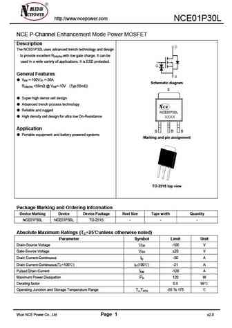
http //www.ncepower.com NCE01P30L NCE P-Channel Enhancement Mode Power MOSFET Description The NCE01P30L uses advanced trench technology and design to provide excellent RDS(ON) with low gate charge. It can be used in a wide variety of applications. It is ESD protested. General Features VDS =-100V,ID =-30A Schematic diagram RDS(ON)
8.10. Size:790K ncepower
nce01p35k.pdf
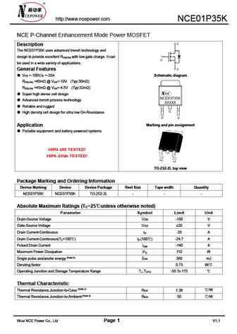
http //www.ncepower.com NCE01P35K NCE P-Channel Enhancement Mode Power MOSFET Description The NCE01P35K uses advanced trench technology and design to provide excellent R with low gate charge. It can DS(ON) be used in a wide variety of applications. General Features V =-100V,I =-35A Schematic diagram DS D R
8.11. Size:307K ncepower
nce01p13.pdf
NCE01P13 http //www.ncepower.com NCE P-Channel Enhancement Mode Power MOSFET Description The NCE01P13 uses advanced trench technology and design to provide excellent RDS(ON) with low gate charge. It can be used in a wide variety of applications. It is ESD protested. General Features VDS =-100V,ID =-13A Schematic diagram RDS(ON)
8.12. Size:325K ncepower
nce01p30d.pdf
http //www.ncepower.com NCE01P30D NCE P-Channel Enhancement Mode Power MOSFET Description The NCE01P30D uses advanced trench technology and design to provide excellent RDS(ON) with low gate charge. It can be used in a wide variety of applications. It is ESD protested. General Features VDS =-100V,ID =-30A RDS(ON)
8.13. Size:400K ncepower
nce01p13k.pdf
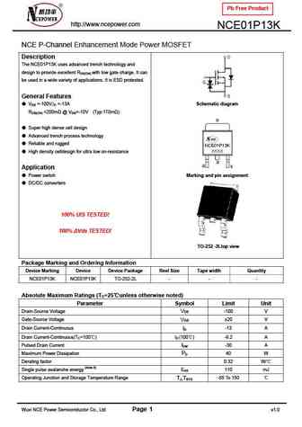
Pb Free Product http //www.ncepower.com NCE01P13K NCE P-Channel Enhancement Mode Power MOSFET Description The NCE01P13K uses advanced trench technology and design to provide excellent RDS(ON) with low gate charge. It can be used in a wide variety of applications. It is ESD protested. General Features VDS =-100V,ID =-13A Schematic diagram RDS(ON)
Otros transistores... NCE0157, NCE0157A2, NCE0157D, NCE01H10, NCE01H10D, NCE01H11, NCE01H13, NCE01H21T, AO3400, NCE01P13K, NCE01P18D, NCE01P18K, NCE01P30, NCE0202M, NCE0202ZA, NCE0208KA, NCE0224