FDC638APZ MOSFET Equivalente. Reemplazo. Hoja de especificaciones. Principales características
Número de Parte: FDC638APZ
Tipo de FET: MOSFET
Polaridad de transistor: P
ESPECIFICACIONES MÁXIMAS
Pdⓘ - Máxima disipación de potencia: 1.6
W
|Vds|ⓘ - Voltaje máximo drenador - fuente: 20
V
|Vgs|ⓘ - Voltaje máximo fuente - puerta: 12
V
|Id|ⓘ - Corriente continua de drenaje: 4.5
A
Tjⓘ - Temperatura máxima de unión: 150
°C
CARACTERÍSTICAS ELÉCTRICAS
trⓘ - Tiempo de subida: 20
nS
Cossⓘ - Capacitancia
de salida: 155
pF
Rds(on)ⓘ - Resistencia estado encendido drenaje a fuente: 0.043
Ohm
Paquete / Cubierta:
SSOT6
Búsqueda de reemplazo de FDC638APZ MOSFET
-
Selección ⓘ de transistores por parámetros
FDC638APZ datasheet
..1. Size:479K fairchild semi
fdc638apz.pdf 
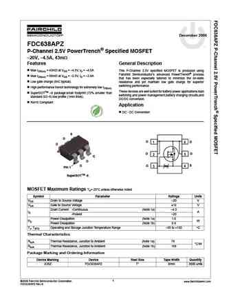
December 2006 FDC638APZ P-Channel 2.5V PowerTrench Specified MOSFET 20V, 4.5A, 43m Features General Description Max rDS(on) = 43m at VGS = 4.5V, ID = 4.5A This P-Channel 2.5V specified MOSFET is produced using Fairchild Semiconductor s advanced PowerTrench process Max rDS(on) = 68m at VGS = 2.5V, ID = 3.8A that has been especially tailored to minim
8.1. Size:154K fairchild semi
fdc638p.pdf
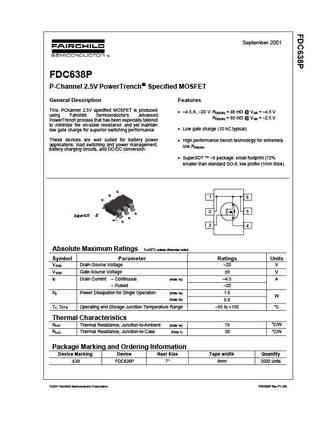
September 2001 FDC638P P-Channel 2.5V PowerTrench Specified MOSFET General Description Features This P 2.5V specified MOSFET is produced -Channel 4.5 A, 20 V. R = 48 m @ V = 4.5 V DS(ON) GS using Fairchild Semiconductor s advanced R = 65 m @ V = 2.5 V DS(ON) GS PowerTrench process that has been especially tailored to minimize the on-state resistanc
8.2. Size:839K cn vbsemi
fdc638p.pdf
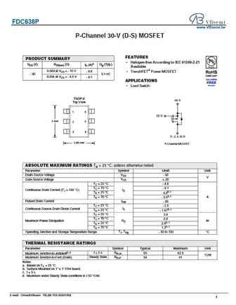
FDC638P www.VBsemi.tw P-Channel 30-V (D-S) MOSFET FEATURES PRODUCT SUMMARY Halogen-free According to IEC 61249-2-21 VDS (V) RDS(on) ( ) ID (A)a Qg (Typ.) Available 0.049 at VGS = - 10 V - 4.8 TrenchFET Power MOSFET - 30 5.1 nC 0.054 at VGS = - 4.5 V - 4.1 APPLICATIONS Load Switch TSOP-6 (4) S Top V iew 1 6 (3) G 3 mm 5 2 3 4 (1, 2, 5, 6) D 2.85 mm P-Cha
9.1. Size:66K fairchild semi
fdc637an.pdf
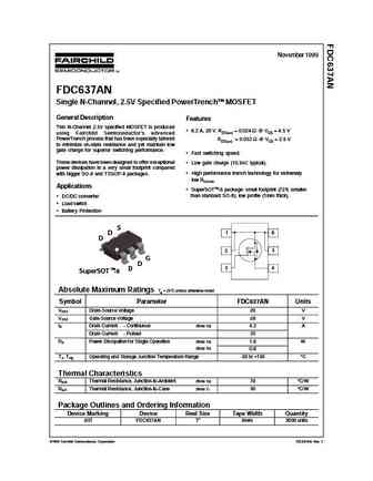
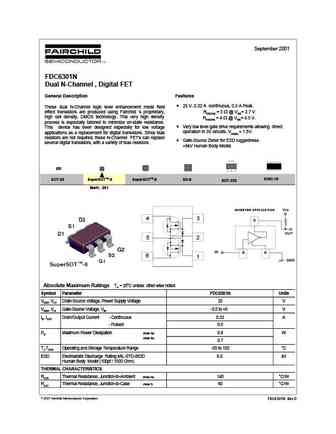
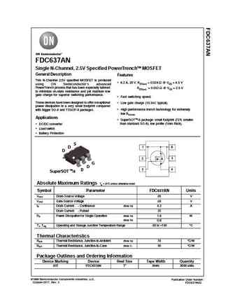
November 1999 FDC637AN Single N-Channel, 2.5V Specified PowerTrenchTM MOSFET General Description Features This N-Channel 2.5V specified MOSFET is produced 6.2 A, 20 V. RDS(on) = 0.024 @ VGS = 4.5 V using Fairchild Semiconductor's advanced PowerTrench process that has been especially tailored RDS(on) = 0.032 @ VGS = 2.5 V to minimize on-state resistance and yet maintain lo
9.2. Size:121K fairchild semi
fdc6323l.pdf
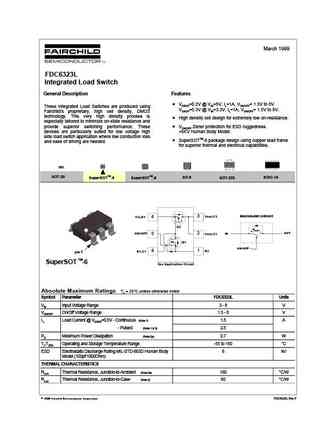
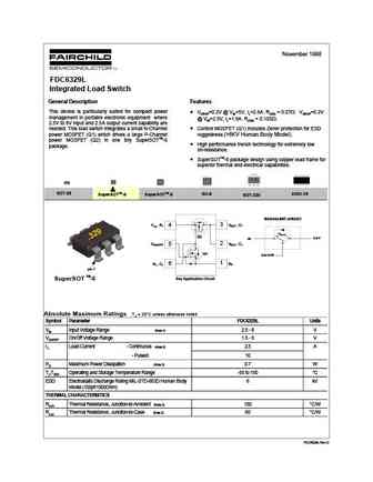
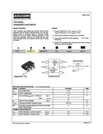
March 1999 FDC6323L Integrated Load Switch General Description Features VDROP=0.2V @ VIN=5V, IL=1A, VON/OFF= 1.5V to 8V These Integrated Load Switches are produced using VDROP=0.3V @ VIN=3.3V, IL=1A, VON/OFF= 1.5V to 8V. Fairchild's proprietary, high cell density, DMOS technology. This very high density process is High density cell design for extremely low on-resistance. especially
9.3. Size:73K fairchild semi
fdc6305n.pdf
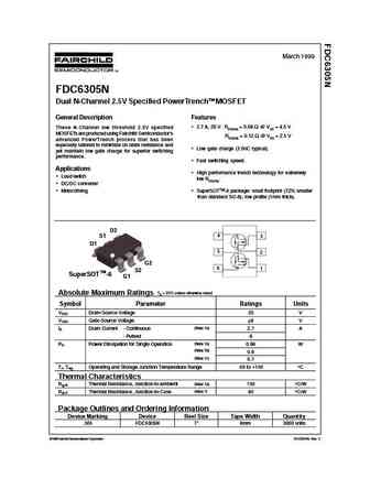
March 1999 FDC6305N Dual N-Channel 2.5V Specified PowerTrenchTM MOSFET General Description Features 2.7 A, 20 V. RDS(ON) = 0.08 @ VGS = 4.5 V These N-Channel low threshold 2.5V specified MOSFETs are produced using Fairchild Semiconductor's RDS(ON) = 0.12 @ VGS = 2.5 V advanced PowerTrench process that has been especially tailored to minimize on-state resistance and Low
9.5. Size:61K fairchild semi
fdc6306p.pdf
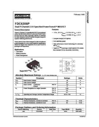
February 1999 FDC6306P Dual P-Channel 2.5V Specified PowerTrench MOSFET Features General Description These P-Channel 2.5V specified MOSFETs are produced -1.9 A, -20 V. RDS(on) = 0.170 @ VGS = -4.5 V using Fairchild Semiconductor's advanced PowerTrench RDS(on) = 0.250 @ VGS = -2.5 V process that has been especially tailored to minimize on-state resistance and yet maintain
9.6. Size:193K fairchild semi
fdc6392s.pdf
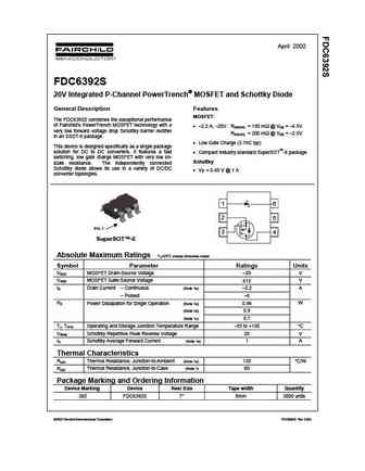
April 2002 FDC6392S 20V Integrated P-Channel PowerTrench MOSFET and Schottky Diode General Description Features MOSFET The FDC6392S combines the exceptional performance of Fairchild's PowerTrench MOSFET technology with a 2.2 A, 20V. RDS(ON) = 150 m @ VGS = 4.5V very low forward voltage drop Schottky barrier rectifier RDS(ON) = 200 m @ VGS
9.7. Size:80K fairchild semi
fdc6304p.pdf
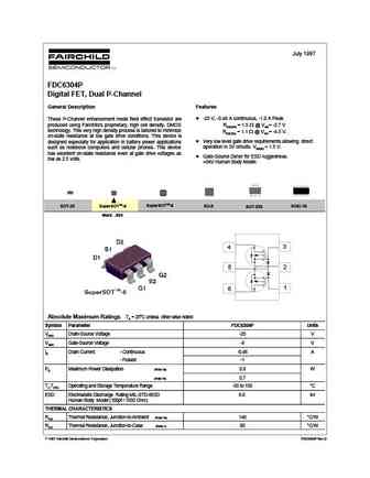
July 1997 FDC6304P Digital FET, Dual P-Channel General Description Features -25 V, -0.46 A continuous, -1.0 A Peak. These P-Channel enhancement mode field effect transistor are produced using Fairchild's proprietary, high cell density, DMOS RDS(ON) = 1.5 @ VGS= -2.7 V technology. This very high density process is tailored to minimize RDS(ON) = 1.1 @ VGS = -4.5 V. on-state
9.8. Size:106K fairchild semi
fdc6320c.pdf
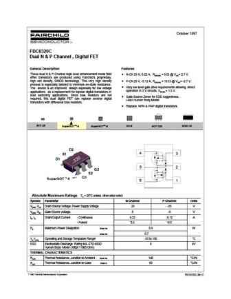
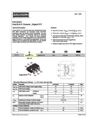
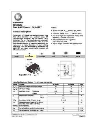
October 1997 FDC6320C Dual N & P Channel , Digital FET General Description Features These dual N & P Channel logic level enhancement mode field N-Ch 25 V, 0.22 A, RDS(ON) = 5 @ VGS= 2.7 V. effec transistors are produced using Fairchild's proprietary, high cell density, DMOS technology. This very high density P-Ch 25 V, -0.12 A, RDS(ON) = 13 @ VGS= -2.7 V. process is especial
9.9. Size:69K fairchild semi
fdc6310p.pdf
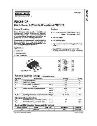
April 2001 FDC6310P Dual P-Channel 2.5V Specified PowerTrench MOSFET General Description Features These P-Channel 2.5V specified MOSFETs are 2.2 A, 20 V. R = 125 m @ V = 4.5 V DS(ON) GS produced using Fairchild Semiconductor's advanced R = 190 m @ V = 2.5 V DS(ON) GS PowerTrench process that has been especially tailored to minimize on-state resistance
9.10. Size:130K fairchild semi
fdc6321c.pdf
April 1999 FDC6321C Dual N & P Channel , Digital FET General Description Features These dual N & P Channel logic level enhancement mode N-Ch 25 V, 0.68 A, RDS(ON) = 0.45 @ VGS= 4.5 V field effect transistors are produced using Fairchild's proprietary, high cell density, DMOS technology. This very P-Ch -25 V, -0.46 A, RDS(ON) = 1.1 @ VGS= -4.5 V. high density process is especi
9.11. Size:82K fairchild semi
fdc6302p.pdf
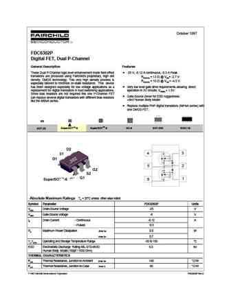
October 1997 FDC6302P Digital FET, Dual P-Channel General Description Features These Dual P-Channel logic level enhancement mode field effect -25 V, -0.12 A continuous, -0.5 A Peak. transistors are produced using Fairchild's proprietary, high cell RDS(ON) = 13 @ VGS= -2.7 V density, DMOS technology. This very high density process is RDS(ON) = 10 @ VGS = -4.5 V. especially
9.12. Size:136K fairchild semi
fdc634p.pdf
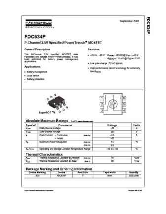
September 2001 FDC634P P-Channel 2.5V Specified PowerTrench MOSFET General Description Features This P-Channel 2.5V specified MOSFET uses 3.5 A, 20 V. R = 80 m @ V = 4.5 V DS(ON) GS Fairchild s low voltage PowerTrench process. It has R = 110 m @ V = 2.5 V DS(ON) GS been optimized for battery power management applications. Low gate charge (7.2 n
9.13. Size:98K fairchild semi
fdc6333c.pdf
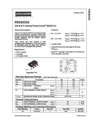
October 2001 FDC6333C 30V N & P-Channel PowerTrench MOSFETs General Description Features These N & P-Channel MOSFETs are produced using Q1 2.5 A, 30V. RDS(ON) = 95 m @ VGS = 10 V Fairchild Semiconductor s advanced PowerTrench RDS(ON) = 150 m @ VGS = 4.5 V process that has been especially tailored to minimize on-state resistance and yet maintain superior Q2 2
9.14. Size:141K fairchild semi
fdc6329l.pdf
November 1998 FDC6329L Integrated Load Switch General Description Features This device is particularly suited for compact power VDROP=0.2V @ VIN=5V, IL=2.8A. R(ON) = 0.07 VDROP=0.2V management in portable electronic equipment where @ VIN=2.5V, IL=1.9A. R(ON) = 0.105 . 2.5V to 8V input and 2.5A output current capability are needed. This load switch integrates a small N-Channel
9.15. Size:374K fairchild semi
fdc6301n.pdf
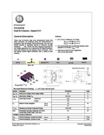
September 2001 FDC6301N Dual N-Channel , Digital FET General Description Features 25 V, 0.22 A continuous, 0.5 A Peak. These dual N-Channel logic level enhancement mode field effect transistors are produced using Fairchild 's proprietary, RDS(ON) = 5 @ VGS= 2.7 V high cell density, DMOS technology. This very high density RDS(ON) = 4 @ VGS= 4.5 V. process is especially tailo
9.16. Size:150K fairchild semi
fdc6308p.pdf
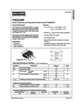
July 1999 FDC6308P Dual P-Channel 2.5V Specified PowerTrenchTM MOSFET General Description Features This P-Channel 2.5V specified MOSFET is a rugged -1.7 A, -18 V. RDS(ON) = 0.18 @ VGS = -4.5 V gate version of Fairchild Semiconductor's advanced RDS(ON) = 0.30 @ VGS = -2.5 V PowerTrench process. It has been optimized for power management applications with a wide range of gate
9.17. Size:149K fairchild semi
fdc6327c.pdf
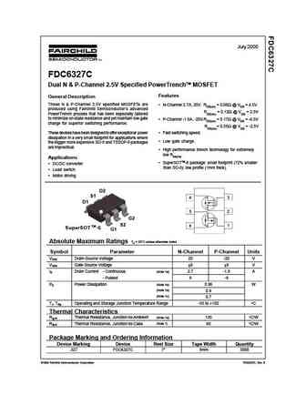
July 2000 FDC6327C Dual N & P-Channel 2.5V Specified PowerTrenchTM MOSFET Features General Description These N & P-Channel 2.5V specified MOSFETs are N-Channel 2.7A, 20V. RDS(on) = 0.08 @ VGS = 4.5V produced using Fairchild Semiconductor's advanced RDS(on) = 0.12 @ VGS = 2.5V PowerTrench process that has been especially tailored to minimize on-state resistance and yet mainta
9.18. Size:61K fairchild semi
fdc633n f095.pdf
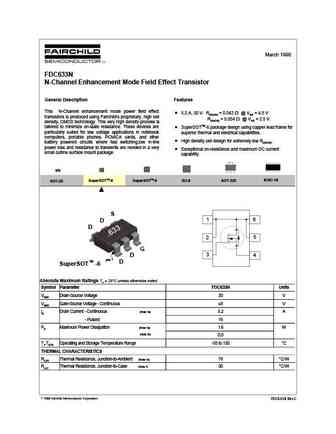
March 1998 FDC633N N-Channel Enhancement Mode Field Effect Transistor General Description Features This N-Channel enhancement mode power field effect 5.2 A, 30 V. RDS(ON) = 0.042 @ VGS = 4.5 V transistors is produced using Fairchild's proprietary, high cell RDS(ON) = 0.054 @ VGS = 2.5 V. density, DMOS technology. This very high density process is tailored to minimize on-stat
9.19. Size:165K fairchild semi
fdc6318p.pdf
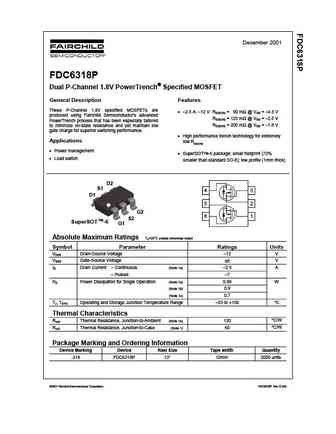
December 2001 FDC6318P Dual P-Channel 1.8V PowerTrench Specified MOSFET General Description Features These P-Channel 1.8V specified MOSFETs are 2.5 A, 12 V. RDS(ON) = 90 m @ VGS = 4.5 V produced using Fairchild Semiconductor's advanced RDS(ON) = 125 m @ VGS = 2.5 V PowerTrench process that has been especially tailored RDS(ON) = 200 m
9.20. Size:78K fairchild semi
fdc6303n.pdf

August 1997 FDC6303N Digital FET, Dual N-Channel General Description Features 25 V, 0.68 A continuous, 2 A Peak. These dual N-Channel logic level enhancement mode field RDS(ON) = 0.6 @ VGS = 2.7 V effect transistors are produced using Fairchild's proprietary, high cell density, DMOS technology. This very high density RDS(ON) = 0.45 @ VGS= 4.5 V. process is especially tailored
9.21. Size:188K fairchild semi
fdc636p.pdf
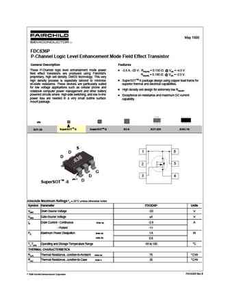
May 1998 FDC636P P-Channel Logic Level Enhancement Mode Field Effect Transistor General Description Features These P-Channel logic level enhancement mode power -2.8 A, -20 V. RDS(ON) = 0.130 @ VGS = -4.5 V field effect transistors are produced using Fairchild's RDS(ON) = 0.180 @ VGS = -2.5 V. proprietary, high cell density, DMOS technology. This very high density process is
9.22. Size:68K fairchild semi
fdc6324l.pdf
March 1999 FDC6324L Integrated Load Switch General Description Features These Integrated Load Switches are produced using Fairchild's VDROP=0.2V @ VIN=12V, IL=1A, VON/OFF=1.5 to 8V proprietary, high cell density, DMOS technology. This very high VDROP=0.3V @ VIN=5V, IL=1A, VON/OFF=1.5 to 8V. density process is especially tailored to minimize on-state High density cell design for extr
9.23. Size:415K fairchild semi
fdc637bnz.pdf

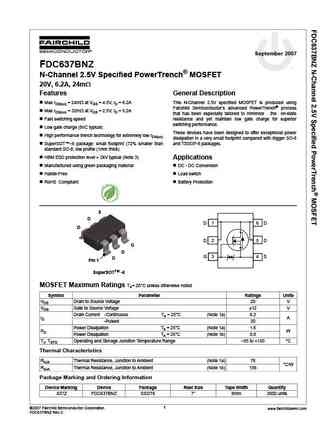
September 2007 FDC637BNZ tm N-Channel 2.5V Specified PowerTrench MOSFET 20V, 6.2A, 24m Features General Description Max rDS(on) = 24m at VGS = 4.5V, ID = 6.2A This N-Channel 2.5V specified MOSFET is produced using Fairchild Semiconductor s advanced PowerTrench process Max rDS(on) = 32m at VGS = 2.5V, ID = 5.2A that has been especially tailored to minimize the on-sta
9.24. Size:365K onsemi
fdc637an.pdf
FDC637AN Single N-Channel, 2.5V Specified PowerTrenchTM MOSFET General Description Features This N-Channel 2.5V specified MOSFET is produced 6.2 A, 20 V. RDS(on) = 0.024 @ VGS = 4.5 V using ON Semiconductor's advanced PowerTrench process that has been especially tailored RDS(on) = 0.032 @ VGS = 2.5 V to minimize on-state resistance and yet maintain low gate charge for
9.25. Size:185K onsemi
fdc6305n.pdf

Is Now Part of To learn more about ON Semiconductor, please visit our website at www.onsemi.com Please note As part of the Fairchild Semiconductor integration, some of the Fairchild orderable part numbers will need to change in order to meet ON Semiconductor s system requirements. Since the ON Semiconductor product management systems do not have the ability to manage part nomenclatur
9.26. Size:204K onsemi
fdc6312p.pdf

Is Now Part of To learn more about ON Semiconductor, please visit our website at www.onsemi.com Please note As part of the Fairchild Semiconductor integration, some of the Fairchild orderable part numbers will need to change in order to meet ON Semiconductor s system requirements. Since the ON Semiconductor product management systems do not have the ability to manage part nomenclatur
9.27. Size:175K onsemi
fdc6306p.pdf

Is Now Part of To learn more about ON Semiconductor, please visit our website at www.onsemi.com Please note As part of the Fairchild Semiconductor integration, some of the Fairchild orderable part numbers will need to change in order to meet ON Semiconductor s system requirements. Since the ON Semiconductor product management systems do not have the ability to manage part nomenclatur
9.28. Size:542K onsemi
fdc6321c.pdf
FDC6321C Dual N & P Channel , Digital FET Features N-Ch 25 V, 0.68 A, RDS(ON) = 0.45 @ VGS= 4.5 V General Description P-Ch -25 V, -0.46 A, RDS(ON) = 1.1 @ VGS= -4.5 V. These dual N & P Channel logic level enhancement mode Very low level gate drive requirements allowing direct field effect transistors are produced using ON operation in 3 V circuits. VGS(th)
9.29. Size:212K onsemi
fdc6333c.pdf

Is Now Part of To learn more about ON Semiconductor, please visit our website at www.onsemi.com Please note As part of the Fairchild Semiconductor integration, some of the Fairchild orderable part numbers will need to change in order to meet ON Semiconductor s system requirements. Since the ON Semiconductor product management systems do not have the ability to manage part nomenclatur
9.30. Size:604K onsemi
fdc6301n.pdf
FDC6301N Dual N-Channel , Digital FET Features General Description 25 V, 0.22 A continuous, 0.5 A Peak. These dual N-Channel logic level enhancement mode field RDS(ON) = 5 @ VGS= 2.7 V effect transistors are produced using ON Semiconductor 's RDS(ON) = 4 @ VGS= 4.5 V. proprietary, high cell density, DMOS technology. This very high density process is especially tailored to
9.31. Size:218K onsemi
fdc6327c.pdf

Is Now Part of To learn more about ON Semiconductor, please visit our website at www.onsemi.com ON Semiconductor and the ON Semiconductor logo are trademarks of Semiconductor Components Industries, LLC dba ON Semiconductor or its subsidiaries in the United States and/or other countries. ON Semiconductor owns the rights to a number of patents, trademarks, copyrights, trade secrets, and oth
9.32. Size:279K onsemi
fdc6318p.pdf

Is Now Part of To learn more about ON Semiconductor, please visit our website at www.onsemi.com Please note As part of the Fairchild Semiconductor integration, some of the Fairchild orderable part numbers will need to change in order to meet ON Semiconductor s system requirements. Since the ON Semiconductor product management systems do not have the ability to manage part nomenclatur
9.33. Size:415K onsemi
fdc637bnz.pdf
September 2007 FDC637BNZ tm N-Channel 2.5V Specified PowerTrench MOSFET 20V, 6.2A, 24m Features General Description Max rDS(on) = 24m at VGS = 4.5V, ID = 6.2A This N-Channel 2.5V specified MOSFET is produced using Fairchild Semiconductor s advanced PowerTrench process Max rDS(on) = 32m at VGS = 2.5V, ID = 5.2A that has been especially tailored to minimize the on-sta
9.34. Size:912K cn vbsemi
fdc637an.pdf
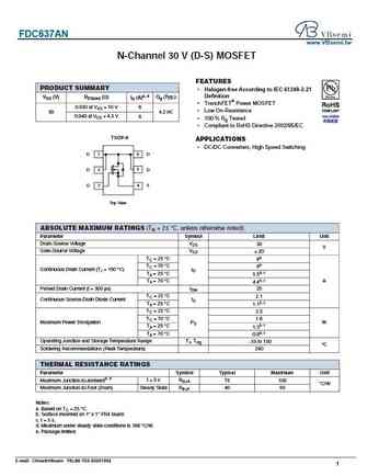
FDC637AN www.VBsemi.tw N-Channel 30 V (D-S) MOSFET FEATURES PRODUCT SUMMARY Halogen-free According to IEC 61249-2-21 Definition VDS (V) RDS(on) ( ) ID (A)a, e Qg (Typ.) TrenchFET Power MOSFET 0.030 at VGS = 10 V 6 Low On-Resistance 30 4.2 nC 0.040 at VGS = 4.5 V 6 100 % Rg Tested Compliant to RoHS Directive 2002/95/EC TSOP-6 APPLICATIONS DC/DC
9.35. Size:2356K cn vbsemi
fdc6305n.pdf
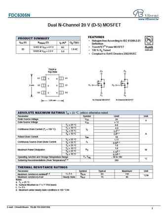
FDC6305N www.VBsemi.tw Dual N-Channel 20 V (D-S) MOSFET FEATURES PRODUCT SUMMARY Halogen-free According to IEC 61249-2-21 VDS (V) RDS(on) ( ) ID (A)a Qg (Typ.) Definition 0.022 at VGS = 4.5 V TrenchFET Power MOSFET 6.0 20 1.8 nC 100 % Rg Tested 0.028 at VGS = 2.5 V 5.0 Compliant to RoHS Directive 2002/95/EC TSOP-6 D1 D 2 D Top View G1 D1 1 6 G 1
9.36. Size:896K cn vbsemi
fdc6312p.pdf
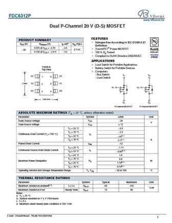
FDC6312P www.VBsemi.tw Dual P-Channel 20 V (D-S) MOSFET FEATURES PRODUCT SUMMARY Halogen-free According to IEC 61249-2-21 VDS (V) RDS(on) ( )ID (A)a Qg (Typ.) Definition 0.075 at VGS = - 4.5V - 4.0 TrenchFET Power MOSFET - 20 2.7 nC 0.100 at VGS = - 2.5 V - 3.2 100 % Rg Tested Compliant to RoHS Directive 2002/95/EC APPLICATIONS Load Switch for Portable Ap
9.37. Size:925K cn vbsemi
fdc6321c.pdf
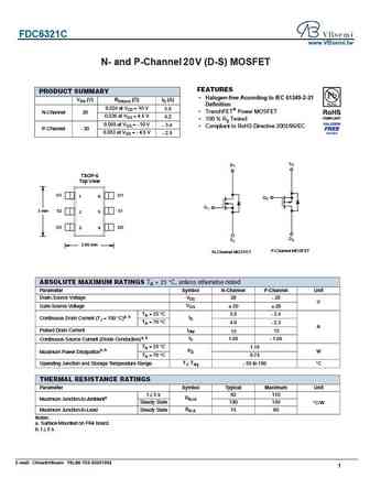
FDC6321C www.VBsemi.tw N- and P-Channel 2 V (D-S) MOSFET 0 FEATURES PRODUCT SUMMARY Halogen-free According to IEC 61249-2-21 VDS (V) RDS(on) ( )ID (A) Definition 0.024 at VGS = 10 V 5.5 TrenchFET Power MOSFET N-Channel 20 0.036 at VGS = 4.5 V 4.2 100 % Rg Tested 0.069 at VGS = - 10 V - 3.4 Compliant to RoHS Directive 2002/95/EC P-Channel - 20 0.083 at V
9.38. Size:925K cn vbsemi
fdc6327c.pdf
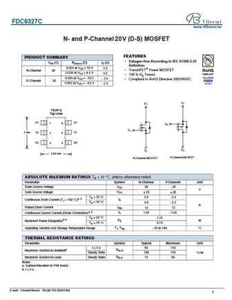
FDC6327C www.VBsemi.tw N- and P-Channel 2 V (D-S) MOSFET 0 FEATURES PRODUCT SUMMARY Halogen-free According to IEC 61249-2-21 VDS (V) RDS(on) ( )ID (A) Definition 0.024 at VGS = 10 V 5.5 TrenchFET Power MOSFET N-Channel 20 0.036 at VGS = 4.5 V 4.2 100 % Rg Tested 0.069 at VGS = - 10 V - 3.4 Compliant to RoHS Directive 2002/95/EC P-Channel - 20 0.083 at V
9.39. Size:861K cn vbsemi
fdc637bnz.pdf
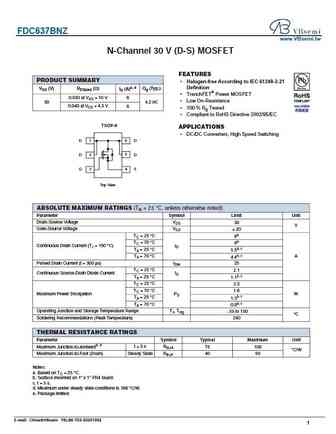
FDC637BNZ www.VBsemi.tw N-Channel 30 V (D-S) MOSFET FEATURES PRODUCT SUMMARY Halogen-free According to IEC 61249-2-21 Definition VDS (V) RDS(on) ( ) ID (A)a, e Qg (Typ.) TrenchFET Power MOSFET 0.030 at VGS = 10 V 6 Low On-Resistance 30 4.2 nC 0.040 at VGS = 4.5 V 6 100 % Rg Tested Compliant to RoHS Directive 2002/95/EC TSOP-6 APPLICATIONS DC/DC
Otros transistores... FDC6321C
, STU3030NLS
, FDC6327C
, STU17L01
, FDC6333C
, STU16L01
, STU15N20
, FDC637BNZ
, 8205A
, FDC6401N
, FDC6420C
, STU15L01
, FDC642P
, FDC642PF085
, FDC655BN
, STU1530PL
, FDC658AP
.