FDC655BN MOSFET Equivalente. Reemplazo. Hoja de especificaciones. Principales características
Número de Parte: FDC655BN
Tipo de FET: MOSFET
Polaridad de transistor: N
ESPECIFICACIONES MÁXIMAS
Pdⓘ - Máxima disipación de potencia: 1.6
W
|Vds|ⓘ - Voltaje máximo drenador - fuente: 30
V
|Vgs|ⓘ - Voltaje máximo fuente - puerta: 20
V
|Id|ⓘ - Corriente continua de drenaje: 6.3
A
Tjⓘ - Temperatura máxima de unión: 150
°C
CARACTERÍSTICAS ELÉCTRICAS
trⓘ - Tiempo de subida: 2
nS
Cossⓘ - Capacitancia
de salida: 100
pF
Rds(on)ⓘ - Resistencia estado encendido drenaje a fuente: 0.025
Ohm
Paquete / Cubierta:
SSOT6
Búsqueda de reemplazo de FDC655BN MOSFET
-
Selección ⓘ de transistores por parámetros
FDC655BN datasheet
..1. Size:253K fairchild semi
fdc655bn.pdf 
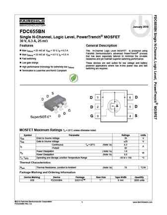
January 2010 FDC655BN tm Single N-Channel, Logic Level, PowerTrench MOSFET 30 V, 6.3 A, 25 m Features General Description Max rDS(on) = 25 m at VGS = 10 V, ID = 6.3 A This N-Channel Logic Level MOSFET is produced using Fairchild Semiconductor s advanced PowerTrench process Max rDS(on) = 33 m at VGS = 4.5 V, ID = 5.5 A that has been especially tailored to minimize t
8.1. Size:188K fairchild semi
fdc655an.pdf
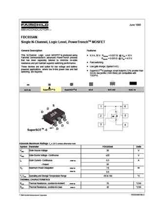
June 1998 FDC655AN Single N-Channel, Logic Level, PowerTrenchTM MOSFET General Description Features This N-Channel Logic Level MOSFET is produced using 6.3 A, 30 V. RDS(ON) = 0.027 @ VGS = 10 V Fairchild Semiconductor's advanced PowerTrench process RDS(ON) = 0.035 @ VGS = 4.5 V. that has been especially tailored to minimize on-state Fast switching. resistance and yet main
9.1. Size:114K fairchild semi
fdc6561an.pdf

April 1999 FDC6561AN Dual N-Channel Logic Level PowerTrenchTM MOSFET General Description Features These N-Channel Logic Level MOSFETs are 2.5 A, 30 V. RDS(ON) = 0.095 @ VGS = 10 V produced using Fairchild Semiconductor's advanced RDS(ON) = 0.145 @ VGS = 4.5 V PowerTrench process that has been especially tailored to minimize the on-state resistance and yet maintain Very fas
9.2. Size:133K fairchild semi
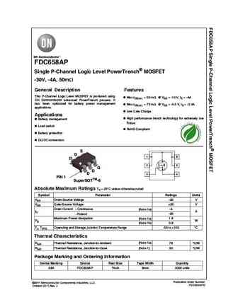
fdc658ap.pdf
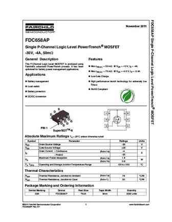
November 2011 FDC658AP Single P-Channel Logic Level PowerTrench MOSFET -30V, -4A, 50m General Description Features This P-Channel Logic Level MOSFET is produced using Max rDS(on) = 50 m @ VGS = -10 V, ID = -4A Fairchild's advanced PowerTrench process. It has been optimized for battery power management applications. Max rDS(on) = 75 m @ VGS = -4.5 V, ID = -3.4A Applications
9.3. Size:116K fairchild semi
fdc654p.pdf
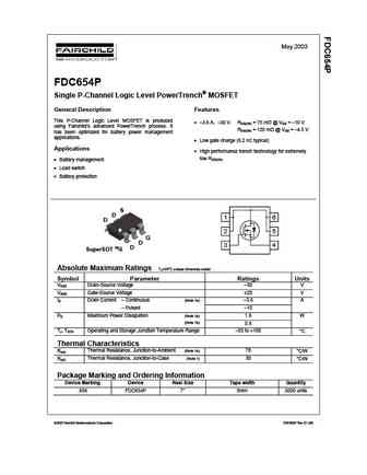
May 2003 FDC654P Single P-Channel Logic Level PowerTrench MOSFET General Description Features This P-Channel Logic Level MOSFET is produced 3.6 A, 30 V. RDS(ON) = 75 m @ VGS = 10 V using Fairchild s advanced PowerTrench process. It RDS(ON) = 125 m @ VGS = 4.5 V has been optimized for battery power management applications. Low gate charge (6.2 nC
9.4. Size:76K fairchild semi
fdc653n.pdf
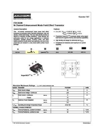
November 1997 FDC653N N-Channel Enhancement Mode Field Effect Transistor General Description Features This N-Channel enhancement mode power field effect 5 A, 30 V. RDS(ON) = 0.035 @ VGS = 10 V transistors is produced using Fairchild's proprietary, high cell RDS(ON) = 0.055 @ VGS = 4.5 V. density, DMOS technology. This very high density process is Proprietary SuperSOTTM-6 pac
9.5. Size:106K fairchild semi
fdc658p.pdf
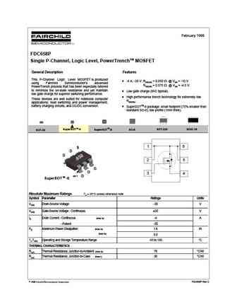
February 1999 FDC658P Single P-Channel, Logic Level, PowerTrenchTM MOSFET General Description Features This P-Channel Logic Level MOSFET is produced -4 A, -30 V. RDS(ON) = 0.050 @ VGS = -10 V using Fairchild Semiconductor's advanced RDS(ON) = 0.075 @ VGS = -4.5 V. PowerTrench process that has been especially tailored to minimize the on-state resistance and yet maintain Lo
9.6. Size:64K fairchild semi
fdc6506p.pdf
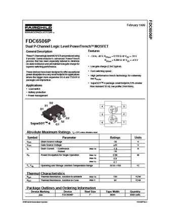
February 1999 FDC6506P Dual P-Channel Logic Level PowerTrench MOSFET Features General Description These P-Channel logic level MOSFETs are produced using -1.8 A, -30 V. RDS(on) = 0.170 @ VGS = -10 V Fairchild Semiconductor's advanced PowerTrench RDS(on) = 0.280 @ VGS = -4.5 V process that has been especially tailored to minimize on-state resistance and yet maintain low g
9.7. Size:257K onsemi
fdc6561an.pdf
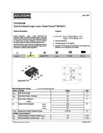
April 1999 FDC6561AN Dual N-Channel Logic Level PowerTrenchTM MOSFET General Description Features These N-Channel Logic Level MOSFETs are 2.5 A, 30 V. RDS(ON) = 0.095 @ VGS = 10 V produced using Fairchild Semiconductor's advanced RDS(ON) = 0.145 @ VGS = 4.5 V PowerTrench process that has been especially tailored to minimize the on-state resistance and yet maintain Very fas
9.8. Size:213K onsemi
fdc658ap.pdf
FDC658AP Single P-Channel Logic Level PowerTrench MOSFET -30V, -4A, 50m General Description Features This P-Channel Logic Level MOSFET is produced using Max rDS(on) = 50 m @ VGS = -10 V, ID = -4A ON Semiconductor advanced PowerTrench process. It has been optimized for battery power management Max rDS(on) = 75 m @ VGS = -4.5 V, ID = -3.4A applications. Low Gate Charge Appli
9.9. Size:73K onsemi
fdc653n.pdf

November 1997 FDC653N N-Channel Enhancement Mode Field Effect Transistor General Description Features This N-Channel enhancement mode power field effect 5 A, 30 V. RDS(ON) = 0.035 @ VGS = 10 V transistors is produced using Fairchild's proprietary, high cell RDS(ON) = 0.055 @ VGS = 4.5 V. density, DMOS technology. This very high density process is Proprietary SuperSOTTM-6 pac
9.10. Size:1873K kexin
fdc658ap.pdf
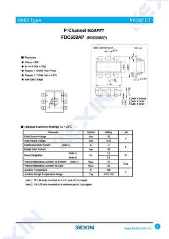
SMD Type MOSFET P-Channel MOSFET FDC658AP (KDC658AP) ( ) SOT-23-6 Unit mm 0.4+0.1 -0.1 Features 6 5 4 VDS (V) =-30V ID =-4 A (VGS =-10V) RDS(ON) 50m (VGS =-10V) 2 3 1 RDS(ON) 75m (VGS =-4.5V) +0.02 0.15 -0.02 +0.01 Low Gate Charge -0.01 +0.2 -0.1 1 6 1.Drain 4.Source 2 5 2.Drain 5.Drain 3.Gate 6.Drain 3 4 Absolute Maximum
9.11. Size:836K cn vbsemi
fdc658ap.pdf
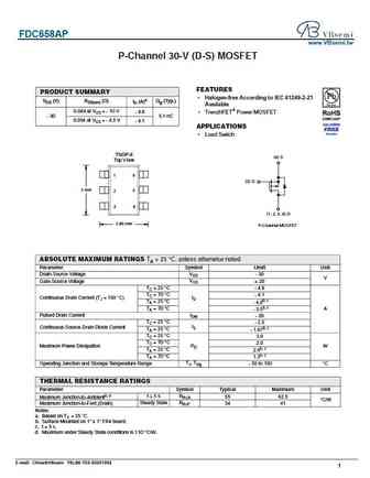
FDC658AP www.VBsemi.tw P-Channel 30-V (D-S) MOSFET FEATURES PRODUCT SUMMARY Halogen-free According to IEC 61249-2-21 VDS (V) RDS(on) ( ) ID (A)a Qg (Typ.) Available 0.049 at VGS = - 10 V - 4.8 TrenchFET Power MOSFET - 30 5.1 nC 0.054 at VGS = - 4.5 V - 4.1 APPLICATIONS Load Switch TSOP-6 (4) S Top V iew 1 6 (3) G 3 mm 5 2 3 4 (1, 2, 5, 6) D 2.85 mm P-Ch
9.12. Size:894K cn vbsemi
fdc6506p.pdf
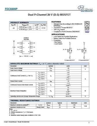
FDC6506P www.VBsemi.tw Dual P-Channel 20 V (D-S) MOSFET FEATURES PRODUCT SUMMARY Halogen-free According to IEC 61249-2-21 VDS (V) RDS(on) ( )ID (A)a Qg (Typ.) Definition 0.075 at VGS = - 4.5V - 4.0 TrenchFET Power MOSFET - 20 2.7 nC 0.100 at VGS = - 2.5 V - 3.2 100 % Rg Tested Compliant to RoHS Directive 2002/95/EC APPLICATIONS Load Switch for Portable Ap
Otros transistores... STU15N20
, FDC637BNZ
, FDC638APZ
, FDC6401N
, FDC6420C
, STU15L01
, FDC642P
, FDC642PF085
, 2SK3878
, STU1530PL
, FDC658AP
, FDC855N
, STU12L01
, FDC8601
, STU10N25
, FDC8602
, STU10N20
.
